

- お役立ち記事
- Fundamentals of LSI testability design and key points of delayed fault testing

その単価は妥当か。
AI が根拠付きで分析。
相見積の比較も発注も進捗管理も、ひとつの画面に。

Fundamentals of LSI testability design and key points of delayed fault testing

目次
Understanding LSI Testability Design
Large Scale Integration (LSI) circuits continue to play a crucial role in the advancement of semiconductor technologies.
With the increasing complexity of these circuits, ensuring their functionality with thorough testing is paramount.
Testability design for LSI circuits aims to make the testing process more efficient, cost-effective, and reliable.
Testability design focuses on incorporating features into an LSI circuit that facilitate its testing.
These features are aimed at simplifying the detection of potential defects that may arise during the manufacturing process.
The process of implementing testability can directly impact the overall quality and performance of the final product.
A well-executed testability design results in reduced testing times, improved fault detection, and increased production yields.
Key Components of Testability Design
Built-In Self-Test (BIST)
One major component of testability design is the utilization of Built-In Self-Test (BIST).
BIST is a mechanism by which a circuit can test itself, using on-chip resources to generate test patterns and analyze results.
This approach allows for continuous and automated testing, eliminating the need for external equipment.
BIST also enhances the flexibility of testing, allowing designers to run tests at various stages of the design and production.
As a result, faults can be identified much earlier in the development process, considerably lowering repair costs.
Scan Design
Another critical component is scan design, where additional circuitry is integrated into the LSI to enhance its testability.
The scan design technique involves inserting scan chains into the circuit.
These chains allow for controllable and observable test points throughout the circuit, without the need to physically probe each element.
By utilizing scan designs, engineers can achieve higher test coverage and ensure that even hard-to-reach faults within the circuit are identifiable.
Scan chains also provide the added advantage of supporting both functional testing and fault isolation during the debug process.
Boundary Scan
Boundary scan, often referred to as IEEE 1149.1 or JTAG, is another significant method utilized in testability design.
It allows for testing the interconnections between chips and the external pins of the device while in circuit.
This method is primarily advantageous for testing highly complex, densely packed PCBs where physical access to pins is challenging.
Boundary scan simplifies the testing of solder bridges and opens, enabling the detection of connectivity issues with ease.
Additionally, it enhances the diagnosis and troubleshooting process for complex digital systems, facilitating the implementation of corrective measures.
Delayed Fault Testing
Delayed fault testing is a technique used for detecting specific types of defects in LSI circuits, particularly those faults that emerge only under particular timing conditions.
These faults, often referred to as “delay faults,” can impair circuit performance even though they occasionally remain undetected through standard testing methods.
Challenges in Delayed Fault Testing
The primary challenge in delayed fault testing is the detection of timing-related faults that only appear under specific operational conditions.
Unlike static functional testing, which deals with logic correctness, delayed fault testing requires proper synchronization with the circuit’s timing specifications.
This type of testing becomes increasingly important in high-frequency circuits where minimal timing drifts can result in significant failures.
Identifying these faults typically demands the use of specialized test pattern generation techniques aimed directly at stressing the circuit’s timing behavior.
Additionally, external noise, variations in power supply, and temperature fluctuations can complicate the detection process, necessitating the use of sophisticated testing equipment.
Approaches to Effective Delayed Fault Testing
Successful delayed fault testing requires an amalgamation of diverse strategies and tools designed to address the unique challenges presented by timing-related defects.
Delay Test Patterns
Designers employ delay test patterns, focusing specifically on path delay or gate delays.
These patterns, once applied to the circuit, induce deliberate delays in element activation, enabling the observation of the circuit’s performance under varying timing conditions.
Designers often use Automatic Test Pattern Generation (ATPG) tools to create these intricate patterns, with emphasis on path sensitization to maximize defect coverage.
Launch-On-Shift and Launch-On-Capture Techniques
For effective testing of both path and gate delays, industry professionals often employ launch-on-shift and launch-on-capture testing techniques.
These techniques utilize scan chains to launch transitions at appropriate times, capturing the resulting output for analysis.
Launch-on-shift relies on the sequential shifting of scan cells, while launch-on-capture activates the transition during a functional clock capture cycle.
Both techniques provide distinct advantages for capturing and diagnosing timing-related faults.
Benefits and Importance of Effective Testing
Incorporating a robust testability design and delayed fault testing strategy ensures the identification of crucial defects early in the LSI production cycle.
These methodologies optimize manufacturing efficiency by reducing the incidence of faulty chips reaching the consumer market.
Moreover, by ensuring high test coverage, manufacturers can produce reliable and high-performance circuits.
This reliability is crucial for maintaining consumer trust, meeting industry standards, and achieving competitive advantage in the fast-paced semiconductor industry.
Effective LSI testability design and delayed fault testing not only determine the success of individual products but also influence an organization’s brand reputation and market positioning.
As the demand for complex semiconductor devices continues to rise, investing in comprehensive testing approaches remains an essential factor for sustained growth and innovation.
この記事の理解を深める
無料ホワイトペーパーをプレゼント
製造業の現場で使える実務資料(PDF)を無料でお届けします。"こんな資料が届きます" ↓ 下のボタンからどうぞ。
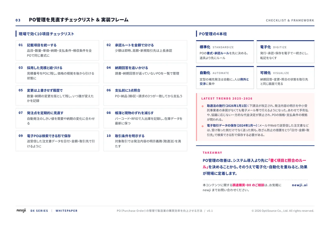
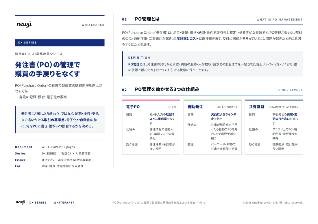
FREE DOCUMENT — サービス資料(PDF・無料)
製造業の見積・受発注クラウド
「Newji one」とは
Newji one は、製造業の調達・受発注に特化したクラウド/AIエージェント。見積依頼・発注書作成・進捗管理・承認をひとつの画面に集約し、AIが比較と異常検知を担当。最後の「GO」だけ人が押す仕組みです。
▶ 製造業の見積・受発注クラウド「Newji one」を、資料で見る(PDF・無料)
- 見積〜発注〜納期を一元管理。催促・転記のムダをゼロに
- AIが相見積もり比較と異常検知。あなたは判断だけに集中
- 取引先は「招待」で完全無料。自社コストだけで取引先ごとデジタル化
※ 取引先から招待された企業様は完全無料でご利用いただけます

 NEWJI総研
 OEM/ODM 生産委託
 AI/DX支援
 見積・発注クラウド Newji one
受発注が増えるほど、入力・確認・催促が重くなる。
受発注管理を“仕組み化“して、ミスと工数を削減しませんか。
見積・発注・納期まで一元管理できます。