

- お役立ち記事
- Effective FPGA design methods and development points: Important know-how for FPGA development

Effective FPGA design methods and development points: Important know-how for FPGA development

目次
Understanding FPGA Design
Field Programmable Gate Arrays, or FPGAs, are integral components in modern electronics, enabling flexibility and adaptability in circuit design.
FPGAs are semiconductor devices that are based around a matrix of configurable logic blocks (CLBs) connected via programmable interconnects.
They can be programmed to perform a multitude of operations, making them a versatile solution for engineers and designers.
Understanding the nature and function of FPGAs is the first step in mastering their design.
Importance of FPGA in Modern Electronics
The increasing demand for rapidly changing electronics has elevated the importance of FPGAs in today’s technological landscape.
FPGAs offer benefits such as parallel processing capability, reconfiguration after deployment, and high performance.
Their role is significant in applications like telecommunications, automotive systems, and data processing.
With FPGAs, developers can adapt to technological advancements without extensive hardware alterations, saving both time and costs.
Strengths of FPGAs
FPGAs are prized for their flexibility.
Unlike ASICs (Application Specific Integrated Circuits), FPGAs can be reprogrammed post-manufacturing.
This reprogrammability allows for updates and improvements without the need for completely new hardware.
Their parallel processing capabilities make them ideal for operations requiring simultaneous processing streams, such as signal processing and image recognition.
Moreover, they offer high-speed performance and the ability to implement complex algorithms efficiently.
Key Design Methods for Effective FPGA Implementation
Creating an effective FPGA design requires a blend of solid planning and attentive execution.
A step-by-step approach helps in aligning the design with the project’s requirements.
Here are some crucial design methods and development points.
Define Requirements Clearly
Before diving into design, it is essential to understand the project’s specific needs.
Defining precise functional and performance requirements lays a solid foundation for subsequent development stages.
Consider factors such as speed, power consumption, and space constraints.
This will guide your selection of the appropriate FPGA model and design structure.
Choose the Right Tools and Technologies
FPGA development is greatly influenced by the tools and technologies chosen at the beginning of the project.
Ensure compatibility between the FPGA device and the toolchain you select.
Tools such as Xilinx Vivado and Intel Quartus Prime are popular for their comprehensive development environments.
These platforms provide simulation, synthesis, and place-and-route capabilities, which are critical for successful design implementation.
Design and Simulate Thoroughly
Design begins with block-level design and schematic entry, progressing to HDL (Hardware Description Language) coding.
Using VHDL or Verilog, define the behavior of the logic gates and complex systems.
After initial design, simulation is vital.
Simulations validate the logic and performance of the design under various conditions.
Fixing logical errors at this stage is less costly compared to post-synthesis revisions.
Iterative Testing and Verification
Following simulation, apply iterative testing to further refine the FPGA design.
Conduct unit tests to confirm each part performs correctly.
Verification is a continuous process, employing static timing analysis and functional verification to ensure performance requirements are met.
Keeping an iterative mindset allows for early identification of design issues and prevents costly rework.
Design Optimization Strategies
Refining the design for efficiency and performance is an ongoing process.
Design optimization strategies focus on minimizing resource usage and enhancing speed and reliability.
Minimize Resource Use
Resource optimization is fundamental, especially in applications with limited space or power.
Analyze the logic and routing resources utilized in the FPGA design.
Simplify redundant processes and combine functions where feasible.
This approach not only saves space but also potentially reduces power consumption and cost.
Improve Timing Performance
Timing closure is often a challenge in FPGA design.
Ensure that all paths meet the timing requirements by optimizing the placement of logic blocks and routing paths.
Use pipelining techniques to improve clock speeds, which enhances the overall data processing rate of the FPGA.
Regularly Review and Update Designs
Technology evolves rapidly, and so should your FPGA design strategies.
Periodic design reviews and updates help incorporate new methodologies and best practices.
Stay informed of advancements in FPGA technology to leverage new features and capabilities.
Conclusion
Effective FPGA design encompasses a thorough understanding of the underlying technology, diligent planning, and precise execution.
By defining clear requirements, utilizing the right tools, and focusing on iterative testing and optimization, engineers can develop robust FPGA solutions that meet the diverse needs of modern applications.
Staying adaptive to new technologies and design techniques ensures a competitive edge in FPGA development, leading to more efficient and effective outcomes.
この記事の理解を深める
無料ホワイトペーパーをプレゼント
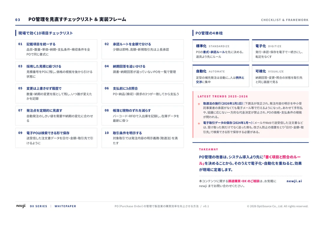
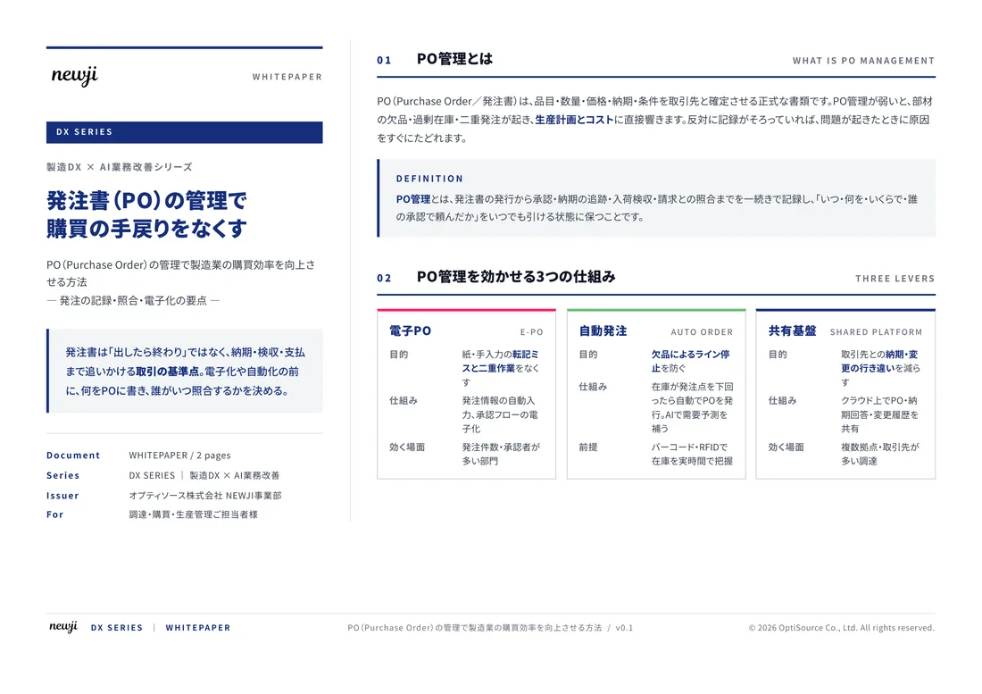
製造業の現場で使える実務資料(PDF)を無料でお届けします。"こんな資料が届きます" ↓ 下のボタンからどうぞ。
FREE DOCUMENT — サービス資料(PDF・無料)
製造業の見積・受発注クラウド
「Newji one」とは
Newji one は、製造業の調達・受発注に特化したクラウド/AIエージェント。見積依頼・発注書作成・進捗管理・承認をひとつの画面に集約し、AIが比較と異常検知を担当。最後の「GO」だけ人が押す仕組みです。
▶ 製造業の見積・受発注クラウド「Newji one」を、資料で見る(PDF・無料)
- 見積〜発注〜納期を一元管理。催促・転記のムダをゼロに
- AIが相見積もり比較と異常検知。あなたは判断だけに集中
- 取引先は「招待」で完全無料。自社コストだけで取引先ごとデジタル化
※ 取引先から招待された企業様は完全無料でご利用いただけます




 NEWJI総研
 OEM/ODM 生産委託
 AI/DX支援
 見積・発注クラウド Newji one
受発注が増えるほど、入力・確認・催促が重くなる。
受発注管理を“仕組み化“して、ミスと工数を削減しませんか。
見積・発注・納期まで一元管理できます。