

- お役立ち記事
- How Are Semiconductors Made? Insights from Industry Experts

その単価は妥当か。
AI が根拠付きで分析。
相見積の比較も発注も進捗管理も、ひとつの画面に。

How Are Semiconductors Made? Insights from Industry Experts

Semiconductors are essential components in modern electronics, and their manufacturing process is both fascinating and complex. Let’s discover how these little wonders are made with insights from industry experts.
目次
Introduction to Semiconductors
Before diving into the manufacturing process, it is crucial to understand what semiconductors are. Semiconductors are materials that have properties between conductors (like metals) and insulators (like glass). This unique characteristic allows them to control electrical currents, making them ideal for use in electronic devices.
The Basic Materials
The most common material used to make semiconductors is silicon. Silicon is abundant, affordable, and has the necessary electronic properties. Other materials like gallium arsenide and germanium are also used but to a lesser extent.
The Manufacturing Process
The manufacturing of semiconductors is often referred to as semiconductor fabrication or “fab.” This intricate process involves several stages, each crucial to the final product.
1. Silicon Wafer Production
The journey begins with the production of silicon wafers. Silicon is extracted from sand and purified to a very high level. The purified silicon is then melted and formed into a large cylindrical ingot. This ingot is sliced into thin discs called wafers. These wafers serve as the substrate for semiconductor devices.
2. Photolithography
Photolithography is the next key step. A protective layer of light-sensitive material, called photoresist, is applied to the silicon wafer. Using ultraviolet light and a photomask, specific patterns are etched onto the wafer, which will determine the layout of the circuits.
3. Etching
Etching removes layers of material from the wafer’s surface to create the desired patterns. There are two main types of etching: wet etching, which uses liquid chemicals, and dry etching, which employs gases. The type of etching depends on the precision required for the semiconductor design.
4. Doping
Doping is the process of adding impurities to the silicon wafer to modify its electrical properties. This step is vital for creating p-type and n-type semiconductors, which are essential for forming transistors. Doping is usually performed through ion implantation or diffusion of dopant gases.
5. Deposition
Deposition involves adding thin layers of different materials to the wafer’s surface. These layers can be insulators, conductors, or additional semiconductors. Techniques like chemical vapor deposition (CVD) and physical vapor deposition (PVD) are used to achieve this.
6. Planarization
Planarization ensures that the wafer’s surface remains flat and smooth. This step is important to maintain the precision of the subsequent processes. Chemical mechanical polishing (CMP) is commonly employed for this task.
7. Metallization
Metallization creates the intricate web of electrical connections between different parts of the semiconductor device. Metals like aluminum or copper are deposited and patterned to form these connections, ensuring that the semiconductor can function as designed.
8. Testing and Packaging
After the manufacturing steps are completed, the wafers undergo rigorous testing to ensure functionality and performance. Any defective units are identified and discarded. The functional semiconductors are then cut from the wafer, encased in protective packaging, and prepared for assembly into electronic devices.
Advancements and Challenges
Innovations in Materials
While silicon continues to dominate the semiconductor industry, new materials are being explored to push the limits of performance. Materials like graphene and carbon nanotubes have the potential to revolutionize the field, offering faster and more efficient semiconductor devices.
Scaling Down Dimensions
One of the ongoing challenges in semiconductor manufacturing is scaling down the dimensions of the components to fit more transistors onto a single chip. This process is known as Moore’s Law, and maintaining its pace requires continuous innovation and precision engineering.
Environmental Impact
The semiconductor industry is not without its environmental challenges. The fabrication process consumes significant energy and produces hazardous waste. Industry experts are actively researching ways to reduce the environmental footprint, such as developing sustainable materials and improving recycling methods.
The Importance of Semiconductors
Semiconductors are the backbone of modern electronics. They power everything from smartphones and computers to medical devices and cars. Their importance in advancing technology cannot be overstated, as they enable the development of smarter, faster, and more efficient devices.
Conclusion
The manufacturing of semiconductors is a complex and fascinating process that involves numerous stages and highly specialized techniques. Understanding this process gives us a greater appreciation of the technology that powers our daily lives. The continuous advancements in materials and manufacturing methods ensure that semiconductors will remain at the forefront of technological innovation for years to come.
この記事の理解を深める
無料ホワイトペーパーをプレゼント
製造業の現場で使える実務資料(PDF)を無料でお届けします。"こんな資料が届きます" ↓ 下のボタンからどうぞ。
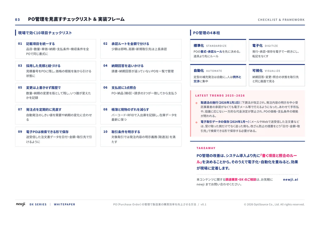
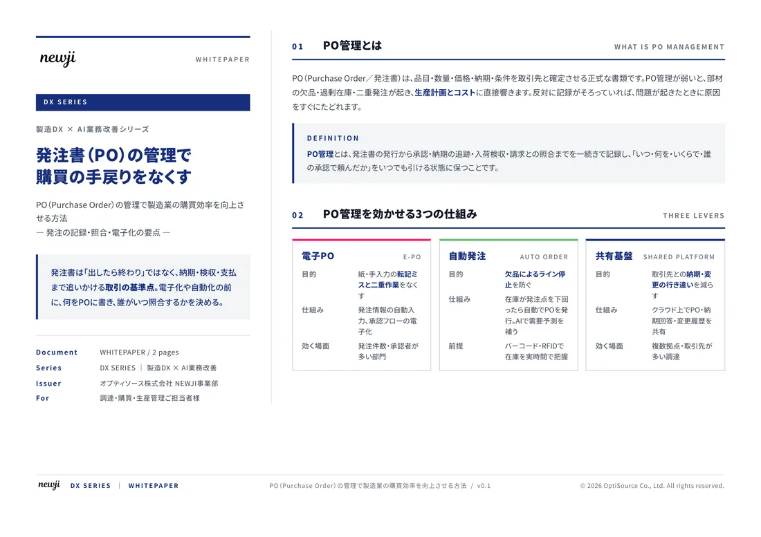
FREE DOCUMENT — サービス資料(PDF・無料)
製造業の見積・受発注クラウド
「Newji one」とは
Newji one は、製造業の調達・受発注に特化したクラウド/AIエージェント。見積依頼・発注書作成・進捗管理・承認をひとつの画面に集約し、AIが比較と異常検知を担当。最後の「GO」だけ人が押す仕組みです。
▶ 製造業の見積・受発注クラウド「Newji one」を、資料で見る(PDF・無料)
- 見積〜発注〜納期を一元管理。催促・転記のムダをゼロに
- AIが相見積もり比較と異常検知。あなたは判断だけに集中
- 取引先は「招待」で完全無料。自社コストだけで取引先ごとデジタル化
※ 取引先から招待された企業様は完全無料でご利用いただけます
関連記事
-

Transforming Modern Electronics: Unleashing the Potential of Silicon-on-Insulator (SOI) Technology for Enhanced Industry Recognition and Market Expansion
-

Silicon Carbideを活用した次世代製造プロセスの最適化方法
-

GAN(敵対的生成ネットワーク)の基礎と実装およびシステム開発への応用
-
PythonとTensorFlow2.0による画像分類、回帰分析、時系列処理と実践プログラミング
-
3D実装技術の基礎と量産実用化に向けた多層配線技術の最新開発動向
-
Pythonによるディープラーニングの基礎と実装ポイント ~デモ付~
 NEWJI総研
 OEM/ODM 生産委託
 AI/DX支援
 見積・発注クラウド Newji one
受発注が増えるほど、入力・確認・催促が重くなる。
受発注管理を“仕組み化“して、ミスと工数を削減しませんか。
見積・発注・納期まで一元管理できます。