

- お役立ち記事
- Evaluation of thin films (electrical/chemical/physical) and analysis methods

スタートアップから大手まで。
調達・受発注をAIで標準化。
相見積比較も進捗管理もAIが下支え。取引先は招待で完全無料。

Evaluation of thin films (electrical/chemical/physical) and analysis methods

目次
Introduction to Thin Film Evaluation
Thin films are integral to the development and functioning of many electronic, optical, and chemical devices.
These films are typically only a few nanometers to a few micrometers thick.
Evaluating the properties of these thin films is crucial to ensure their efficiency and reliability.
The assessment of thin films revolves around understanding their electrical, chemical, and physical characteristics.
Different analysis techniques help in determining the quality and performance of these films in various applications.
Electrical Evaluation of Thin Films
Electrical analysis of thin films primarily focuses on their conductivity, resistivity, and dielectric properties.
Conductivity
Conductivity is a measure of a material’s ability to conduct electric current.
Thin films, especially those used in semiconductors and solar cells, need to have a specific level of conductivity to function effectively.
Techniques like the four-point probe method and Hall effect measurements are common for assessing conductivity in thin films.
Resistivity
Resistivity is the resistance to the flow of electric current and is crucial for understanding the efficiency of thin films in electronic devices.
Measuring resistivity helps in determining how well a thin film can control electricity.
Techniques such as the van der Pauw method are often used for this purpose.
Dielectric Properties
Dielectric properties are important for thin films used in capacitors and other electronic applications.
These properties influence how the film stores and releases electric energy.
Impedance spectroscopy is a common technique for evaluating the dielectric properties of thin films.
Chemical Evaluation of Thin Films
Chemical analysis of thin films is essential to understand their composition and how they interact with their environment.
Composition Analysis
Knowing the exact chemical makeup of a thin film is important for ensuring its performance and stability.
Techniques such as X-ray photoelectron spectroscopy (XPS) and energy-dispersive X-ray spectroscopy (EDX) are commonly used to analyze the chemical composition.
Environmental Stability
Thin films need to be stable under various environmental conditions to be effective in their applications.
Chemically evaluating the environmental stability of thin films helps in predicting their longevity and performance.
Techniques such as Fourier-transform infrared spectroscopy (FTIR) can be used to study the environmental stability of thin films.
Corrosion and Oxidation Resistance
For thin films used in harsh or reactive environments, assessing their resistance to corrosion and oxidation is vital.
This evaluation helps in selecting suitable films that can withstand such conditions for longer periods.
Electrochemical techniques like cyclic voltammetry can provide insights into the corrosion and oxidation resistance of thin films.
Physical Evaluation of Thin Films
Physical properties of thin films such as thickness, adhesion, and morphology significantly affect their performance.
Thickness Measurement
The thickness of a thin film is a critical factor influencing its electrical and optical properties.
Techniques like ellipsometry and atomic force microscopy (AFM) are widely used for precise thickness measurements.
Adhesion Strength
Adhesion strength determines how well a thin film can remain attached to its substrate without peeling or cracking.
Assessing adhesion is crucial for films that are subject to mechanical stress.
Pull-off tests and scratch tests are common methods to evaluate the adhesion strength of thin films.
Morphology and Surface Roughness
The surface morphology and roughness of a thin film can affect its application, especially in optics and electronics.
Atomic force microscopy (AFM) and scanning electron microscopy (SEM) are powerful techniques for analyzing the surface morphology and roughness.
Advanced Analysis Methods
As technology advances, so do the methods for analyzing thin films.
These advanced techniques provide a more comprehensive understanding of thin films beyond basic evaluations.
Raman Spectroscopy
Raman spectroscopy is a non-destructive technique used to gain insight into the vibrational modes of molecules within a thin film.
This method can be used to assess the molecular composition and structural properties.
X-ray Diffraction (XRD)
XRD is a powerful method for investigating the crystallographic structure of thin films.
It helps in determining phase identification and other structural components integral to thin film applications.
Secondary Ion Mass Spectrometry (SIMS)
SIMS allows for the detailed analysis of the atomic composition of thin films.
It is particularly useful for depth profiling, giving insights into the distribution of elements within the film.
Conclusion
Evaluating the electrical, chemical, and physical properties of thin films is essential for improving and optimizing their performance in various applications.
With a range of analysis techniques available, it is possible to gain a comprehensive understanding of the capabilities and limitations of different thin films.
Continued advancements in these analysis methods are vital for the ongoing innovation and development in technologies that rely on thin film applications.
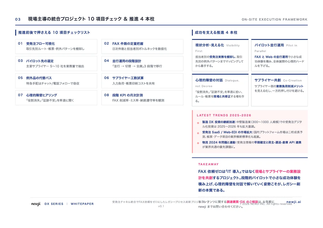
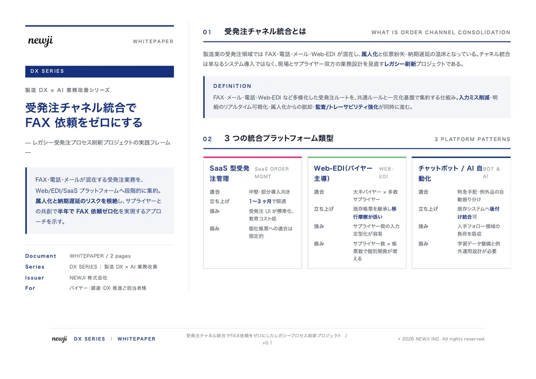
この記事の理解を深める
無料ホワイトペーパーをプレゼント
製造業の現場で使える実務資料(PDF)を無料でお届けします。"こんな資料が届きます" ↓ 下のボタンからどうぞ。
PRODUCT — 製造業向け 調達・受発注クラウド
この記事の課題、
newji で解決しませんか?
newji は、製造業の調達・受発注に特化したクラウド/AIエージェント。見積依頼・発注書作成・進捗管理・承認をひとつの画面に集約し、AIが比較と異常検知を担当。最後の「GO」だけ人が押す仕組みです。
- 見積〜発注〜納期を一元管理。催促・転記のムダをゼロに
- AIが相見積もり比較と異常検知。あなたは判断だけに集中
- 取引先は「招待」で完全無料。自社コストだけで取引先ごとデジタル化
※ 取引先から招待された企業様は完全無料でご利用いただけます



 調達購買アウトソーシング
 OEM/ODM 生産委託
 NEWJI DX
 受発注AIエージェント