

- お役立ち記事
- Fundamentals of FPGA circuit design, trouble prevention measures, and application to improving design quality

その単価は妥当か。
AI が根拠付きで分析。
相見積の比較も発注も進捗管理も、ひとつの画面に。

Fundamentals of FPGA circuit design, trouble prevention measures, and application to improving design quality

目次
Understanding FPGA Circuit Design
Field Programmable Gate Arrays (FPGAs) are highly versatile and reprogrammable integrated circuits that offer immense flexibility in digital circuit design.
Unlike traditional chips, FPGAs can be configured after manufacturing, allowing designers to implement various digital functions and optimize their systems.
To harness the full potential of FPGAs, understanding the fundamentals of its circuit design is crucial.
Basic Concepts of FPGA
An FPGA comprises an array of programmable logic blocks, interconnected by a vast number of reconfigurable gates.
These devices include elements like lookup tables, flip-flops, multiplexers, and more.
At the heart of FPGA design is the ability to customize these elements to perform specific functionalities.
Design begins with describing the desired functionality using a hardware description language (HDL) like VHDL or Verilog.
The HDL code is then synthesized into a logic circuit, which is subsequently mapped onto the FPGA architecture.
This process involves defining inputs, outputs, and the behavior of data flows through these configurable blocks.
The Design Workflow
The FPGA design workflow is typically composed of several key steps:
1. **Specification**: Define the requirements and specifications of the desired system.
2. **Design Entry**: Develop the HDL code and create the block diagram.
3. **Synthesis**: Convert the HDL code into a gate-level netlist.
4. **Implementation**: Map the design onto the FPGA, optimizing the use of logic elements.
5. **Simulation**: Conduct a thorough simulation to verify the design meets all specifications.
6. **Testing and Debugging**: Implement the design within a real FPGA and test under real-world conditions.
Efficient management of this workflow ensures that potential design errors are minimized, resulting in a high-quality, reliable circuit.
Preventing Troubles in FPGA Design
The adaptability of FPGAs provides remarkable advantages but also presents potential pitfalls if not handled correctly.
Prevention measures are crucial to avoid common issues such as timing errors, resource wastage, and unexpected behavior.
Understanding Timing Constraints
Proper management of timing constraints is essential in FPGA design to prevent bottlenecks and latency issues.
This involves defining the clock frequency and ensuring signal paths are optimized for propagation delay.
Timing analysis tools can be leveraged to perform static checks and identify violations before physical testing.
Setting realistic constraints early in development helps avoid lengthy redesigns.
Efficient Resource Utilization
FPGA resources, such as logic elements, memory blocks, and I/O pins, need to be utilized efficiently to maximize performance without exceeding the device’s capacity.
Careful planning and optimization of algorithms help in minimizing resource consumption.
This includes reusing components, employing efficient coding techniques, and choosing the right FPGA with adequate resources for the intended application.
Verification and Validation
Verification is integral to ensuring the design performs as intended under all possible conditions.
Both simulation and in-system testing are essential to validate functionality.
Continuous integration techniques, such as version control and automated testing, help track changes and catch errors early.
Incorporating rigorous validation processes avoids costly errors later in development.
Applying FPGA Design to Improve Quality
The flexible nature of FPGAs offers great opportunities to enhance design quality and meet modern technological demands.
Custom Design Optimization
FPGAs allow for specific customization tailored to application needs, which leads to more efficient solutions compared to fixed-function chips.
By refining algorithms and logic paths, designers can achieve lower power consumption, higher speed, and reduced latency.
The iterative nature of FPGA design enables continuous improvements, enhancing overall design quality.
Scalability and Adaptability
FPGA designs allow for scalable and adaptable solutions, accommodating fast-paced technological advancements.
This is particularly beneficial in fields such as automotive, telecommunications, and consumer electronics, where market demands evolve rapidly.
By incorporating scalable modules and future-proof architectures, products remain relevant and competitive over time.
Prototyping and Innovation
FPGAs provide an excellent platform for prototyping and experimenting with new ideas.
Their reconfigurable nature makes them ideal for evaluating different design options before committing to more expensive custom ASIC development.
This supports innovation, allowing designers to explore cutting-edge technologies, such as artificial intelligence and machine learning applications, within an FPGA framework.
By grasping the fundamentals of FPGA design, implementing preventive measures, and leveraging the adaptable nature of FPGAs, designers can significantly improve the quality, reliability, and performance of their digital systems.
Understanding these principles sets the foundation for successful FPGA circuit design and contributes to robust innovations in multiple industrial applications.
この記事の理解を深める
無料ホワイトペーパーをプレゼント
製造業の現場で使える実務資料(PDF)を無料でお届けします。"こんな資料が届きます" ↓ 下のボタンからどうぞ。
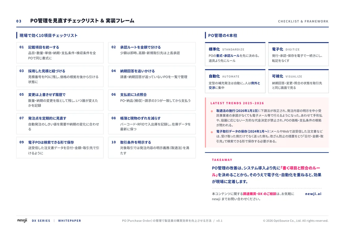
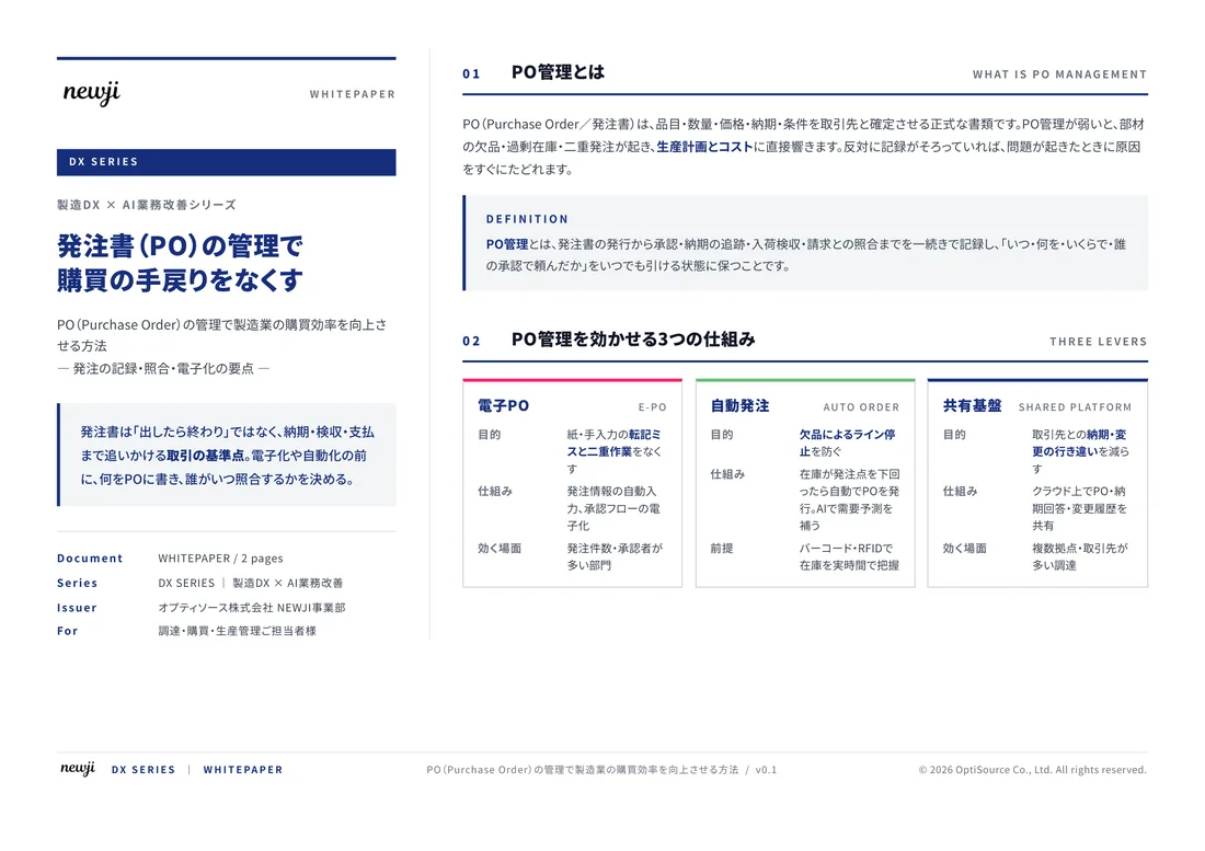
FREE DOCUMENT — サービス資料(PDF・無料)
製造業の見積・受発注クラウド
「Newji one」とは
Newji one は、製造業の調達・受発注に特化したクラウド/AIエージェント。見積依頼・発注書作成・進捗管理・承認をひとつの画面に集約し、AIが比較と異常検知を担当。最後の「GO」だけ人が押す仕組みです。
▶ 製造業の見積・受発注クラウド「Newji one」を、資料で見る(PDF・無料)
- 見積〜発注〜納期を一元管理。催促・転記のムダをゼロに
- AIが相見積もり比較と異常検知。あなたは判断だけに集中
- 取引先は「招待」で完全無料。自社コストだけで取引先ごとデジタル化
※ 取引先から招待された企業様は完全無料でご利用いただけます




 NEWJI総研
 OEM/ODM 生産委託
 AI/DX支援
 見積・発注クラウド Newji one
受発注が増えるほど、入力・確認・催促が重くなる。
受発注管理を“仕組み化“して、ミスと工数を削減しませんか。
見積・発注・納期まで一元管理できます。