

- お役立ち記事
- Fundamentals of sputtering, trouble prevention measures, and quality improvement/improvement measures

Fundamentals of sputtering, trouble prevention measures, and quality improvement/improvement measures

目次
Understanding the Basics of Sputtering
Sputtering is a widely used technique in the field of material science for depositing thin films onto various substrates.
This process plays a crucial role in the manufacturing of semiconductors, solar panels, and various types of coatings.
At its core, sputtering involves the ejection of atoms from a target material, which are then deposited onto a substrate surface.
The process takes place in a vacuum environment to enhance the quality and adherence of the coating.
The main components of a sputtering system include a vacuum chamber, target material, substrate holder, and power source.
How Sputtering Works
The sputtering process begins when a high-energy particle, often from an inert gas like argon, collides with the target material.
This collision causes atoms to be ejected from the target.
These ejected atoms travel through the vacuum and eventually settle on the substrate, forming a thin film layer.
The choice of target material is vital, as it determines the composition of the thin film.
Materials must be selected based on the desired properties of the final product, such as electrical conductivity, optical transparency, or wear resistance.
Optimizing Sputtering Parameters
Several parameters influence the quality and efficiency of the sputtering process.
One key factor is the pressure within the vacuum chamber.
Maintaining an optimal pressure level is essential to control the energy of the sputtering gas ions and the deposition rate of the atoms.
Another factor is the power applied to the target material.
Higher power levels increase the rate of sputtering, but can also lead to increased stress in the thin film.
Finding the right balance is crucial to avoid defects and ensure uniform coating.
Temperature is also important, as it affects the adhesion and structure of the thin film.
Each material has an optimal deposition temperature that promotes better bonding and minimizes stresses.
Choosing the Right Sputtering Technique
There are various sputtering techniques depending on the application needs, including DC sputtering, RF sputtering, and magnetron sputtering.
DC sputtering is simple and cost-effective, suitable for conductive materials.
RF sputtering is ideal for insulating materials, as it uses alternating current to maintain plasma stability.
Magnetron sputtering uses magnetic fields to trap electrons near the target material, enhancing the efficiency of the process and allowing for higher deposition rates.
Selecting the appropriate technique involves evaluating factors such as material type, desired film quality, and production speed.
Preventing Sputtering Issues
Even with optimal parameters, sputtering processes can encounter several issues that impact quality and consistency.
Knowing how to prevent these problems is crucial to maintaining efficient operations and high-quality output.
Contamination Control
One common issue in sputtering processes is contamination, where foreign particles mix with the target material, leading to impure films.
To prevent contamination, it is essential to clean all components thoroughly before starting the sputtering process.
Regular maintenance of the vacuum chamber and filtration systems is also necessary to remove any accumulated contaminants.
Arcing and Particle Accumulation
Arcing, a disruptive electrical discharge, can damage both the target and the substrate, affecting film quality.
Arcing can be minimized by using proper grounding techniques and ensuring clean surfaces to prevent electrical imbalances.
Particle accumulation on the substrate can lead to defects in the thin film.
Using shield plates and optimizing the deposition angles can help reduce this risk, as it prevents particles from directly striking the substrate.
Improving Sputtering Quality
For manufacturers and researchers, improving the quality of sputtered films is an ongoing goal.
Several strategies can be implemented to enhance the results achieved through sputtering processes.
Substrate Preparation and Selection
Proper substrate preparation can greatly enhance the adherence and uniformity of the thin film.
Cleaning the substrate’s surface and removing any oxidation or organic residues are critical first steps.
Choosing the right substrate material is also important.
Materials should be chosen based on compatibility with the target material, thermal expansion coefficients, and intended application of the film.
Advanced Process Control
Employing advanced process control methods, such as real-time monitoring systems, can significantly improve sputtering quality.
These systems provide feedback on critical parameters like film thickness, uniformity, and deposition rate.
With real-time data, operators can make necessary adjustments promptly, ensuring consistent output and minimizing defects.
Layer Structuring
Layer structuring is a method that involves depositing multiple layers with varied materials or properties to enhance film performance.
For instance, applying a protective layer over a conductive layer can improve the durability and functionality of the thin film.
By strategically designing multilayer structures, manufacturers can meet specific application requirements and improve the overall quality of the sputtered film.
Conclusion
Sputtering is a versatile and essential technique in creating thin films for a multitude of applications.
Understanding its fundamentals, knowing how to prevent issues, and employing quality improvement strategies are critical for achieving optimal results.
By controlling sputtering parameters, preventing contamination, and leveraging advanced techniques, manufacturers can produce high-performance films that meet current and future demands.
With continuing advancements in sputtering technology, the possibilities for innovation and quality enhancement are virtually limitless.
この記事の理解を深める
無料ホワイトペーパーをプレゼント
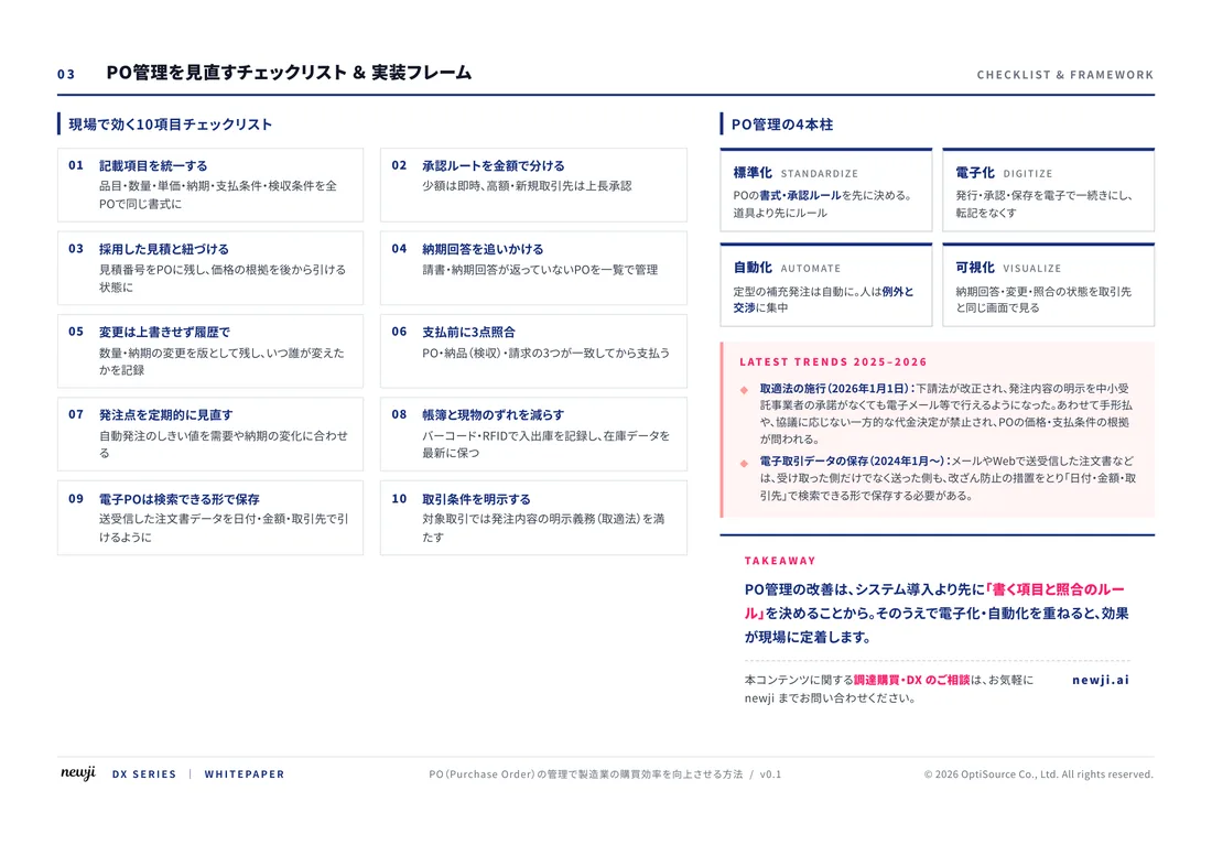
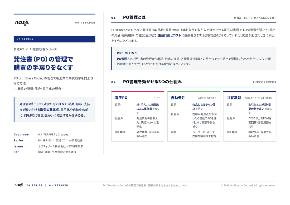
製造業の現場で使える実務資料(PDF)を無料でお届けします。"こんな資料が届きます" ↓ 下のボタンからどうぞ。
FREE DOCUMENT — サービス資料(PDF・無料)
製造業の見積・受発注クラウド
「Newji one」とは
Newji one は、製造業の調達・受発注に特化したクラウド/AIエージェント。見積依頼・発注書作成・進捗管理・承認をひとつの画面に集約し、AIが比較と異常検知を担当。最後の「GO」だけ人が押す仕組みです。
▶ 製造業の見積・受発注クラウド「Newji one」を、資料で見る(PDF・無料)
- 見積〜発注〜納期を一元管理。催促・転記のムダをゼロに
- AIが相見積もり比較と異常検知。あなたは判断だけに集中
- 取引先は「招待」で完全無料。自社コストだけで取引先ごとデジタル化
※ 取引先から招待された企業様は完全無料でご利用いただけます
関連記事
-

Transforming Modern Electronics: Unleashing the Potential of Silicon-on-Insulator (SOI) Technology for Enhanced Industry Recognition and Market Expansion
-

製造業調達購買部門が知っておくべきOSI参照モデルの基礎と応用
-

ALD(原子層堆積)/ALE(原子層エッチング)技術の基礎と高機能薄膜への応用
-

革新的PVD技術で製造業が変わる!未来の生産現場を探る
-
ALD/ALE技術の原理と応用
-
OSI参照モデル(OSI Reference Model)を理解して製造業のネットワークを最適化する
 NEWJI総研
 OEM/ODM 生産委託
 AI/DX支援
 見積・発注クラウド Newji one
受発注が増えるほど、入力・確認・催促が重くなる。
受発注管理を“仕組み化“して、ミスと工数を削減しませんか。
見積・発注・納期まで一元管理できます。