

- お役立ち記事
- Circuit mounting technology and high-temperature mounting technology to maximize the performance of next-generation power semiconductors

その単価は妥当か。
AI が根拠付きで分析。
相見積の比較も発注も進捗管理も、ひとつの画面に。

Circuit mounting technology and high-temperature mounting technology to maximize the performance of next-generation power semiconductors

Next-generation power semiconductors hold the promise of transforming the electronics industry with their superior performance, efficiency, and capability to handle high voltages and frequencies.
However, to harness their full potential, understanding and implementing the right circuit mounting and high-temperature mounting technologies are crucial.
These techniques ensure that the semiconductors perform optimally, providing durability and reliability in various applications.
目次
Understanding Circuit Mounting Technology
Circuit mounting technology refers to the process by which semiconductor devices are attached to printed circuit boards (PCBs) or other substrates.
As power semiconductors evolve, the need for advanced mounting techniques becomes more critical, ensuring that these components are efficiently integrated into various systems.
Importance of Circuit Mounting
Proper circuit mounting is essential for optimal performance of power semiconductors.
It affects thermal management, electrical connectivity, and mechanical stability.
Poor mounting techniques can lead to overheating, electrical resistance, or mechanical failure, ultimately reducing the lifespan and efficiency of the semiconductor.
Types of Circuit Mounting Technologies
Several technologies are employed for circuit mounting, including:
1. **Surface Mount Technology (SMT)**: This method involves placing components directly onto the surface of PCBs.
It is widely used due to its cost-effectiveness and efficiency in handling high-density circuits.
2. **Through-Hole Mounting**: Components are inserted into holes drilled into the PCB and soldered in place.
While not as common for high-frequency applications, it provides strong mechanical bonds, which is beneficial for components that experience physical stress.
3. **Chip-on-Board (COB)**: This involves mounting bare semiconductor chips directly onto the PCB, offering excellent electrical performance and space-saving advantages.
COB is often used in applications requiring compact and efficient designs.
Addressing Thermal Challenges with Circuit Mounting
One of the primary concerns in circuit mounting is managing the heat generated by power semiconductors during operation.
Efficient thermal management ensures that these components perform optimally and do not degrade prematurely.
Thermal Management Techniques
Effective thermal management is achieved through a combination of design considerations and mounting materials.
1. **Heat Sinks**: Attaching heat sinks to semiconductors aids in dissipating heat away from the device, thus reducing the operating temperature and enhancing longevity.
2. **Thermal Interface Materials (TIMs)**: These materials are used between the semiconductor and heat sinks to improve thermal transfer.
TIMs fill in microscopic air gaps, allowing more efficient heat conduction.
3. **Efficient Layout Design**: The circuit’s physical layout can significantly impact thermal management.
Placing components strategically and utilizing materials with high thermal conductivity can effectively reduce hotspots.
High-Temperature Mounting Technologies
With advancements in power semiconductors, there is a growing need for components to operate reliably at higher temperatures.
This requires mounting technologies that can withstand and function effectively under extreme thermal conditions.
Challenges in High-Temperature Mounting
High temperatures can cause several issues, including thermal expansion, warping, and breakdown of materials.
Components must be mounted using techniques and materials that can handle these stresses without degrading.
Advanced Materials and Methods
Innovative materials and methods are being developed to address high-temperature operational requirements.
1. **High-Temperature Soldering**: Special solder materials that can withstand higher temperatures without melting are used.
These solders maintain electrical connections even in harsh conditions.
2. **Metal Ceramic Substrates**: These substrates have excellent thermal conductivity and can endure high temperatures.
They are increasingly used in high-power applications to ensure effective thermal dissipation.
3. **Thermal Cycling and Shock Resistance**: Mounting methodologies are designed to resist thermal cycling (repeated rapid temperature changes) and thermal shock, preventing mechanical failures in semiconductors.
Maximizing Performance with Integrated Solutions
To fully exploit the capabilities of next-generation power semiconductors, integrated solutions that combine circuit and high-temperature mounting technologies are essential.
This integrated approach ensures that semiconductors operate efficiently across various applications and environments.
Customized Mounting Solutions
Tailoring mounting solutions to specific applications can significantly enhance performance.
Customization involves selecting the right combination of materials and techniques to meet the operational demands of the semiconductor.
Proactive Design and Testing
Incorporating circuit and high-temperature mounting technologies from the initial design phase ensures smoother integration and fewer issues during operation.
Comprehensive testing under simulated operating conditions is crucial to identify potential problems early and optimize design solutions.
The Future of Power Semiconductor Mounting Technologies
As the electronics industry continues to push boundaries, mounting technologies must evolve to support semiconductor advancements.
Future technologies will focus on further enhancing thermal management, reliability, and mechanical stability in increasingly compact and efficient designs.
Emphasis on Sustainability
With growing environmental concerns, there is also a need for sustainable and eco-friendly materials and processes in mounting technologies.
This includes developing methods that reduce waste and energy consumption during manufacturing and disposal.
Continued Research and Development
Ongoing research and development in materials science and engineering will drive innovations in mounting technologies.
Collaboration between semiconductor manufacturers, research institutions, and industries will be vital in overcoming future challenges.
In conclusion, as next-generation power semiconductors become integral to modern electronics, implementing advanced circuit and high-temperature mounting technologies is imperative.
By addressing thermal challenges, employing innovative materials, and integrating customized solutions, the performance and reliability of these semiconductors can be maximized, paving the way for more efficient and durable electronic devices.
この記事の理解を深める
無料ホワイトペーパーをプレゼント
製造業の現場で使える実務資料(PDF)を無料でお届けします。"こんな資料が届きます" ↓ 下のボタンからどうぞ。
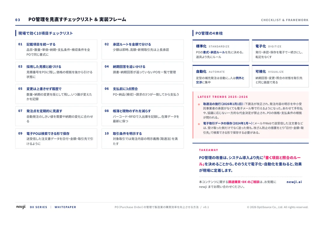
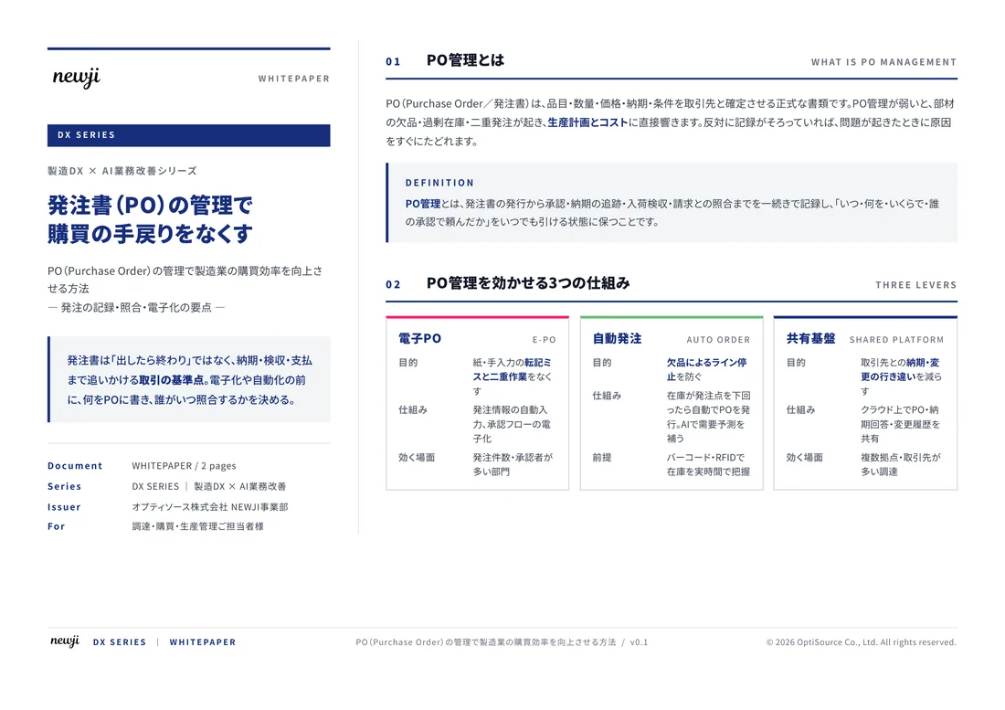
FREE DOCUMENT — サービス資料(PDF・無料)
製造業の見積・受発注クラウド
「Newji one」とは
Newji one は、製造業の調達・受発注に特化したクラウド/AIエージェント。見積依頼・発注書作成・進捗管理・承認をひとつの画面に集約し、AIが比較と異常検知を担当。最後の「GO」だけ人が押す仕組みです。
▶ 製造業の見積・受発注クラウド「Newji one」を、資料で見る(PDF・無料)
- 見積〜発注〜納期を一元管理。催促・転記のムダをゼロに
- AIが相見積もり比較と異常検知。あなたは判断だけに集中
- 取引先は「招待」で完全無料。自社コストだけで取引先ごとデジタル化
※ 取引先から招待された企業様は完全無料でご利用いただけます
関連記事
-

Transforming Modern Electronics: Unleashing the Potential of Silicon-on-Insulator (SOI) Technology for Enhanced Industry Recognition and Market Expansion
-

Building a Digital Infrastructure to Support the Next Generation of Manufacturing
-

Power Appsで作る!簡易的な工場巡回アプリ
-
Power Automateで挑戦!製造業務フローの自動化
-
Shift to next generation manufacturing Potential of blockchain
-
Power BIで始める!製造業KPIダッシュボードの作成
 NEWJI総研
 OEM/ODM 生産委託
 AI/DX支援
 見積・発注クラウド Newji one
受発注が増えるほど、入力・確認・催促が重くなる。
受発注管理を“仕組み化“して、ミスと工数を削減しませんか。
見積・発注・納期まで一元管理できます。