

- お役立ち記事
- Basics of semiconductor packaging and the latest technologies of SiP, WLP, FOWLP, and TSV

Basics of semiconductor packaging and the latest technologies of SiP, WLP, FOWLP, and TSV

目次
Understanding Semiconductor Packaging
Semiconductor packaging is a critical step in the manufacturing process of electronic devices.
It involves enclosing the tiny and delicate semiconductor components within a protective housing to ensure their functionality and reliability.
Packaging not only safeguards the semiconductor chip but also provides connections to the external environment, facilitating the operation of electronic devices.
Semiconductor packaging plays a vital role in the technological advancement of electronics.
It impacts the performance, power efficiency, and overall size of the devices.
In essence, packaging bridges the gap between the silicon die and the external circuitry.
As such, advancements in semiconductor packaging are crucial for the evolution of modern electronics.
The Role of System-in-Package (SiP)
One of the most significant advancements in semiconductor packaging is the System-in-Package (SiP) technology.
SiP refers to an assembly of multiple integrated circuits (ICs) packaged together to function as a complete system.
This packaging method allows for a higher level of integration, enabling more complex and capable electronic devices in a smaller form factor.
SiP offers several advantages, such as improved performance, reduced power consumption, and cost savings.
By integrating components like sensors, processors, and memory into a single package, SiP enables the creation of compact and efficient systems that can power a variety of applications, from mobile devices to IoT gadgets.
Furthermore, SiP technology allows for greater flexibility in design, enabling manufacturers to customize solutions according to specific needs.
It enables quick adaptation to new technologies and innovations, ultimately speeding up the product development cycle.
Wafer-Level Packaging (WLP): A Closer Look
Wafer-Level Packaging (WLP) is another revolutionary approach in the semiconductor industry.
Unlike traditional packaging methods, WLP processes the entire wafer instead of individual dies, streamlining manufacturing and reducing costs.
WLP offers several significant advantages.
Firstly, it allows for more compact and lightweight devices due to the elimination of bulky packaging elements.
This is particularly advantageous in consumer electronics, where size and weight are critical factors.
Additionally, WLP enhances thermal performance as it allows better heat dissipation at the device level.
The reduced thermal resistance extends the lifespan of the components and improves reliability.
WLP is also known for its enhanced electrical performance as it provides shorter interconnect paths, minimizing signal delays and enhancing overall device performance.
The ease of testing and increased throughput achieved by processing the whole wafer further adds to WLP’s appeal.
The Emergence of Fan-Out Wafer-Level Packaging (FOWLP)
Fan-Out Wafer-Level Packaging (FOWLP) is a variant of WLP that addresses some limitations of the traditional approach.
FOWLP involves redistributing the I/O connections beyond the dimensions of the die, effectively “fanning out” the connections to provide more space for interconnections.
This packaging innovation enables better electrical performance, owing to shorter and more efficient interconnect paths.
FOWLP facilitates higher routing density, allowing more functionality to be packed into a single package.
This technology is widely used in applications where miniaturization and high performance are critical, such as in smartphones and wearable devices.
Additionally, FOWLP is cost-effective due to its efficient use of materials and streamlined manufacturing process.
As the demand for smaller, faster, and more efficient electronic devices continues to rise, FOWLP stands out as a desirable solution for meeting these needs.
Through-Silicon Via (TSV) Technology
Through-Silicon Via (TSV) technology is another integral aspect of modern semiconductor packaging.
TSV involves creating vertical electrical connections that pass through the silicon wafer itself, allowing for 3D integration of multiple dies.
TSV technology enhances performance by reducing the length of intra-package connections, resulting in faster signal transmission and reduced power consumption.
This is particularly advantageous in high-performance computing and data centers, where energy efficiency and speed are paramount.
Furthermore, TSV enables higher integration density, effectively doubling or tripling the functionality within the same package footprint.
This makes it possible to pack more processing power and memory into an integrated circuit, making TSV an ideal choice for advanced applications such as artificial intelligence and machine learning.
The Future of Semiconductor Packaging
The semiconductor industry is always evolving, and packaging technologies continue to be at the forefront of this evolution.
As the demand for smaller, faster, and more efficient electronics grows, innovation in semiconductor packaging will play an increasingly crucial role.
In the future, we can expect to see more advancements in materials, processes, and design methodologies.
New materials with better thermal and electrical properties will likely be developed, complementing the existing technologies.
Additionally, advancements in artificial intelligence and machine learning may bring about new design methodologies, optimizing the packaging process for various applications.
Moreover, as the Internet of Things (IoT) and 5G technologies continue to expand, semiconductor packaging will have to accommodate the increased demands of these systems.
Packaging technologies that enable higher data rates and improved power efficiency will become increasingly important as connectivity becomes ubiquitous.
Conclusion
Semiconductor packaging is a vital component of electronics manufacturing, impacting the performance, cost, and reliability of devices.
Technologies like SiP, WLP, FOWLP, and TSV have revolutionized the way we design and produce semiconductor packages, allowing for greater integration, improved performance, and a reduction in size and power consumption.
As technology advances, so too will packaging innovations, shaping the future of electronics and enabling the creation of more sophisticated and capable devices.
As we look ahead, continued research and development in semiconductor packaging will be essential for meeting the ever-changing demands of the electronics industry.
この記事の理解を深める
無料ホワイトペーパーをプレゼント
製造業の現場で使える実務資料(PDF)を無料でお届けします。"こんな資料が届きます" ↓ 下のボタンからどうぞ。
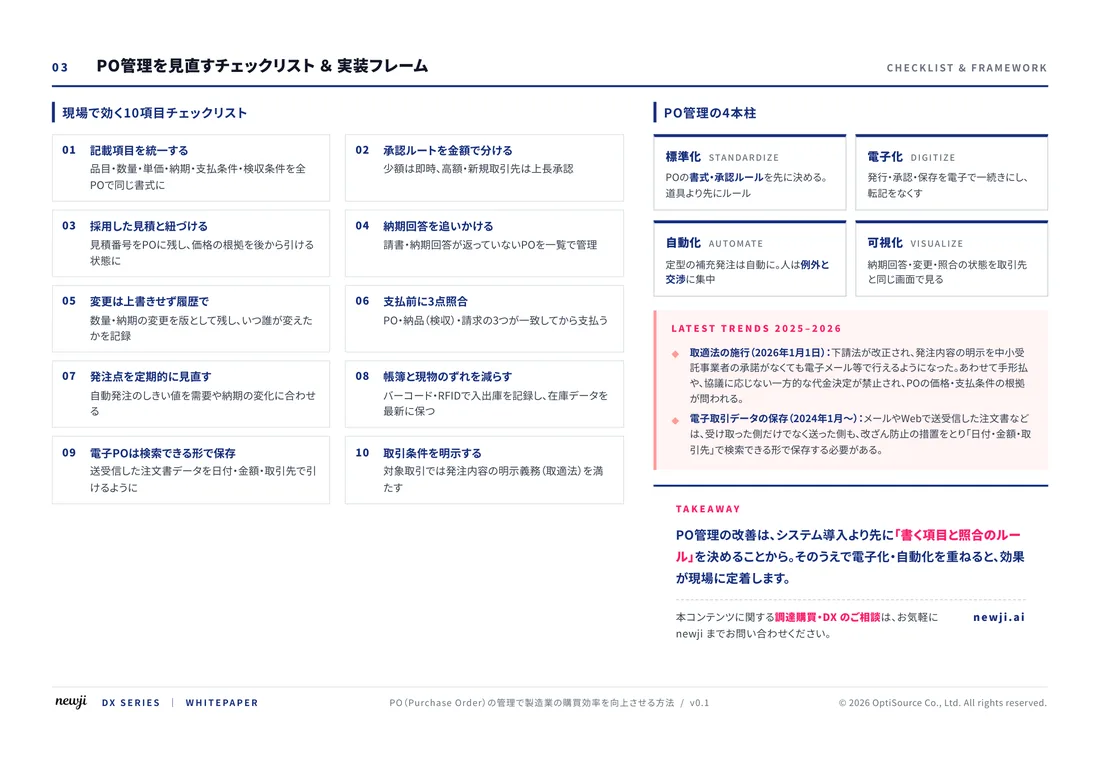
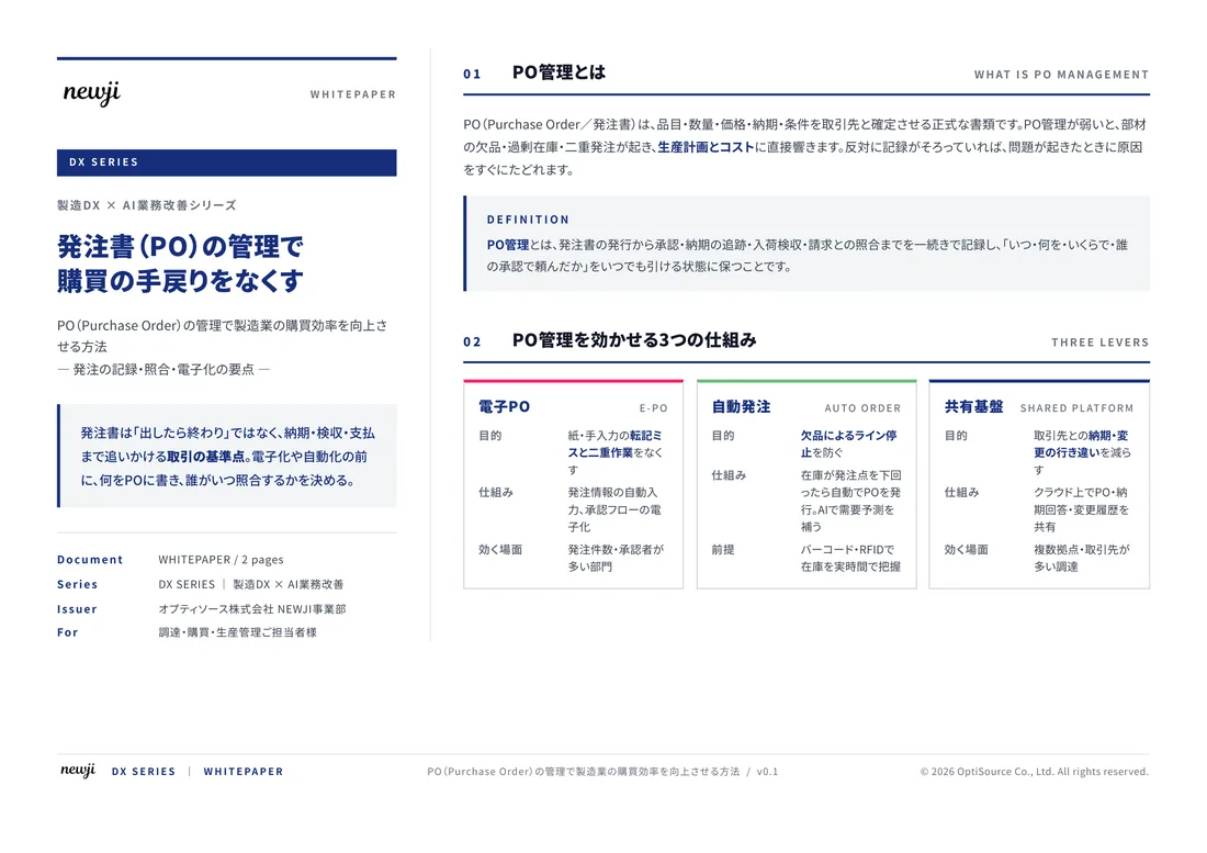
FREE DOCUMENT — サービス資料(PDF・無料)
製造業の見積・受発注クラウド
「Newji one」とは
Newji one は、製造業の調達・受発注に特化したクラウド/AIエージェント。見積依頼・発注書作成・進捗管理・承認をひとつの画面に集約し、AIが比較と異常検知を担当。最後の「GO」だけ人が押す仕組みです。
▶ 製造業の見積・受発注クラウド「Newji one」を、資料で見る(PDF・無料)
- 見積〜発注〜納期を一元管理。催促・転記のムダをゼロに
- AIが相見積もり比較と異常検知。あなたは判断だけに集中
- 取引先は「招待」で完全無料。自社コストだけで取引先ごとデジタル化
※ 取引先から招待された企業様は完全無料でご利用いただけます
関連記事
-

FO-WLP/PLPとは:半導体パッケージの基本
-
半導体パッケージの基礎とSiP、WLP、FOWLP、TSVの最新技術
-

Transforming Modern Electronics: Unleashing the Potential of Silicon-on-Insulator (SOI) Technology for Enhanced Industry Recognition and Market Expansion
-
FOWLPの市場性から分類デザインプロセス応用将来まで全てを解説
-
FOWLPファンアウトウエハレベルパッケージの基礎と最新技術
-

Silicon Carbideを活用した次世代製造プロセスの最適化方法
 NEWJI総研
 OEM/ODM 生産委託
 AI/DX支援
 見積・発注クラウド Newji one
受発注が増えるほど、入力・確認・催促が重くなる。
受発注管理を“仕組み化“して、ミスと工数を削減しませんか。
見積・発注・納期まで一元管理できます。