

- お役立ち記事
- Development of next-generation clean room antifouling paint and application in the semiconductor manufacturing equipment market

Development of next-generation clean room antifouling paint and application in the semiconductor manufacturing equipment market

目次
Introduction to Clean Room Antifouling Paint
In the world of semiconductor manufacturing, maintaining a contamination-free environment is crucial.
Clean rooms, spaces specially designed to regulate environmental factors like dust particles and microbial contamination, are vital in preserving the integrity of semiconductor devices.
The latest innovation aiding in this endeavor is the development of next-generation clean room antifouling paint.
This paint is engineered to prevent the buildup of contaminants on surfaces, thus enhancing the effectiveness and efficiency of semiconductor production.
The significance of antifouling technology in maintaining ultra-clean environments cannot be overstated.
The advanced properties of these paints help in minimizing maintenance time and costs while increasing the overall yield of semiconductor production processes.
What is Clean Room Antifouling Paint?
Clean room antifouling paint is a specialized coating designed to inhibit the growth and accumulation of biological and chemical contaminants.
Unlike regular paints, antifouling paints create a surface resistant to pollutants and microorganisms that can interfere with sensitive equipment and processes.
The nature of semiconductor manufacturing means that even the tiniest particle or microorganism can disrupt production, affecting both quality and efficiency.
By applying an antifouling coating, manufacturers can ensure cleaner surfaces, reducing the risk of contamination and consequent downtime or defects.
How Does Clean Room Antifouling Paint Work?
Antifouling paint works through a combination of physical and chemical mechanisms to prevent contaminants from adhering to surfaces.
The paints often contain specialized polymers that create a smooth and slippery finish, deterring particles from sticking.
Additionally, some formulations incorporate antimicrobial agents that actively prevent the growth of bacteria and fungi.
These coatings are typically formulated to be anti-static, meaning they repel dust and other particles that might otherwise be attracted by static electricity.
By maintaining static-neutral surfaces, clean room antifouling paint minimizes the accumulation of particles that could compromise semiconductor fabrication.
Technology Behind the Paint
The innovative technology behind these paints involves complex chemistry and material science.
Advanced formulations are developed using state-of-the-art materials like modified silicones and fluoropolymers known for their low surface energy properties.
These substances create a microscopic barrier that makes it difficult for contaminants to attach to surfaces.
Another key aspect of the technology is the paint’s durability.
Antifouling paints must withstand regular cleaning procedures and exposure to various chemical agents used in semiconductor production.
Therefore, robust binding agents are used to ensure the paint’s longevity and effectiveness over time.
Benefits of Antifouling Paints in Semiconductor Manufacturing
Implementing antifouling paints in clean rooms offers numerous benefits, directly impacting the semiconductor industry’s success.
These benefits include improved cleanliness and hygiene, reduced maintenance intervals, and enhanced productivity.
Enhanced Cleanliness and Hygiene
By choosing antifouling paint, semiconductor manufacturers significantly improve the cleanliness and hygiene of their clean rooms.
The paint’s properties help prevent contamination by providing a physical barrier to particles and microorganisms.
This results in less frequent cleaning requirements and minimizes the risk of contamination-related issues.
Reduced Maintenance
Because antifouling painted surfaces require less frequent cleaning and upkeep, maintenance costs and times are significantly reduced.
Regular maintenance downtimes are shortened, allowing continuous workflow and reducing production delays.
This not only enhances efficiency but also extends the lifespan of clean room facilities and equipment.
Improved Productivity
With cleaner and more reliable surfaces, production performance is enhanced.
Fewer contaminants mean fewer defects in semiconductor products, resulting in a higher yield of usable devices.
Consequently, manufacturing processes become more efficient, and the quality of output improves.
This leads to substantial cost savings and a stronger competitive position in the market.
Future Applications and Market Impact
As the semiconductor industry continues to evolve and grow, the demand for effective antifouling solutions is set to increase.
The need to adopt next-generation clean room antifouling paints will only become more pressing to meet stringent industry standards and consumer expectations.
Potential for Market Expansion
While the initial application of these paints has been primarily within the semiconductor industry, there’s potential for expansion into other critical sectors.
Industries such as pharmaceuticals, biotechnology, and aerospace, which also rely heavily on ultra-clean environments, could benefit from similar antifouling technologies.
Development Trends and Innovations
Innovation in antifouling technologies continues, with ongoing research focused on enhancing the properties of these paints.
Future developments may involve even more sophisticated materials capable of self-cleaning or more effective microbial resistance.
Additionally, industry partnerships may advance the technology further, integrating antifouling solutions into wider industrial applications.
Conclusion
The development of next-generation clean room antifouling paint marks a significant stride forward in enhancing semiconductor manufacturing efficiency.
By providing a durable and effective solution to contamination challenges, these paints play a crucial role in maintaining high standards of production.
As the semiconductor sector continues to grow and evolve, the importance of advanced antifouling technologies cannot be overstated.
Looking to the future, the expansion and innovation of these antifouling solutions seem promising, with potential applications extending to other high-tech industries.
Embracing these advancements can help ensure cleaner, safer, and more productive manufacturing environments worldwide.
この記事の理解を深める
無料ホワイトペーパーをプレゼント
製造業の現場で使える実務資料(PDF)を無料でお届けします。"こんな資料が届きます" ↓ 下のボタンからどうぞ。
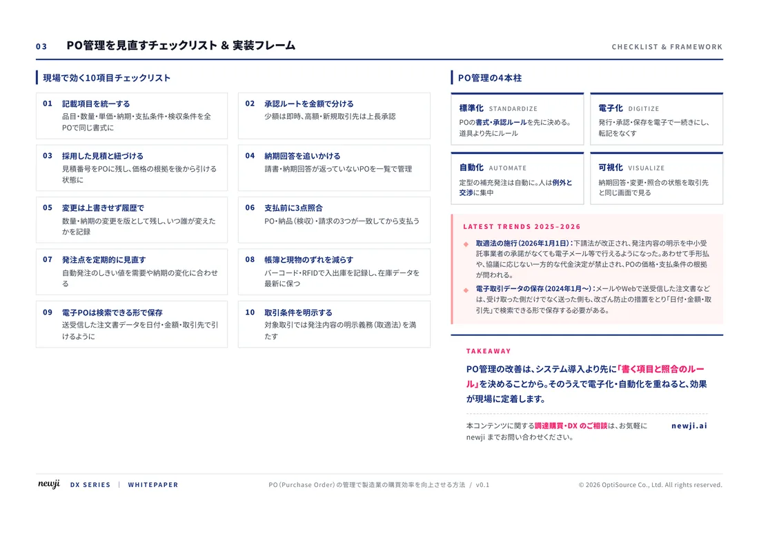
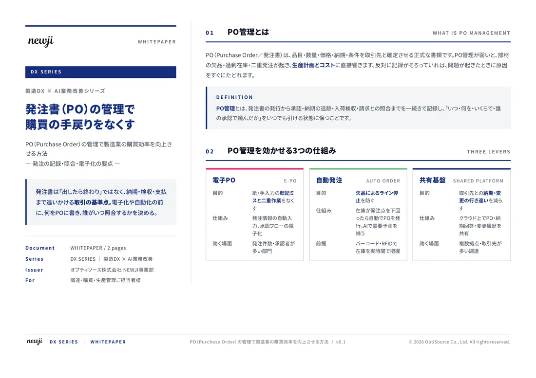
FREE DOCUMENT — サービス資料(PDF・無料)
製造業の見積・受発注クラウド
「Newji one」とは
Newji one は、製造業の調達・受発注に特化したクラウド/AIエージェント。見積依頼・発注書作成・進捗管理・承認をひとつの画面に集約し、AIが比較と異常検知を担当。最後の「GO」だけ人が押す仕組みです。
▶ 製造業の見積・受発注クラウド「Newji one」を、資料で見る(PDF・無料)
- 見積〜発注〜納期を一元管理。催促・転記のムダをゼロに
- AIが相見積もり比較と異常検知。あなたは判断だけに集中
- 取引先は「招待」で完全無料。自社コストだけで取引先ごとデジタル化
※ 取引先から招待された企業様は完全無料でご利用いただけます
関連記事
-

粒子フィルタの基礎とPythonによる時系列データ解析実践講座
-
クリーンルーム(Clean Room)の重要性と製造業での最適な設計方法
-

Self-Cleaning Glassの未来: 調達購買部門が知っておくべき革新と導入のメリット
-

Transforming Modern Electronics: Unleashing the Potential of Silicon-on-Insulator (SOI) Technology for Enhanced Industry Recognition and Market Expansion
-

Building a Digital Infrastructure to Support the Next Generation of Manufacturing
-
Shift to next generation manufacturing Potential of blockchain
 NEWJI総研
 OEM/ODM 生産委託
 AI/DX支援
 見積・発注クラウド Newji one
受発注が増えるほど、入力・確認・催促が重くなる。
受発注管理を“仕組み化“して、ミスと工数を削減しませんか。
見積・発注・納期まで一元管理できます。