

- お役立ち記事
- For process engineers in the electronics manufacturing industry! How to optimize printed circuit board manufacturing with inkjet technology

スタートアップから大手まで。
調達・受発注をAIで標準化。
相見積比較も進捗管理もAIが下支え。取引先は招待で完全無料。

For process engineers in the electronics manufacturing industry! How to optimize printed circuit board manufacturing with inkjet technology

目次
Introduction to Inkjet Technology in PCB Manufacturing
Printed circuit board (PCB) manufacturing is a crucial aspect of the electronics industry, where efficiency and precision are of paramount importance.
Among the innovative technologies transforming this landscape, inkjet technology stands out as a game-changer, offering significant improvements in manufacturing processes.
Understanding how to harness inkjet technology can greatly benefit process engineers in optimizing PCB production.
Inkjet technology, originally developed for the printing industry, has found its way into PCB manufacturing due to its unique advantages.
It involves depositing precise amounts of conductive and insulating materials onto a substrate to create the intricate patterns required for electronic circuits.
This method offers a high degree of accuracy and flexibility compared to traditional PCB manufacturing processes.
The Advantages of Inkjet Technology for PCB Manufacturing
Precision and Accuracy
One of the primary advantages of inkjet technology is its superior precision and accuracy.
In PCB manufacturing, even minor imperfections can lead to faulty circuits and device malfunctions.
Inkjet technology allows for precise control over the deposition of materials, ensuring that every detail of the circuit design is accurately represented.
Reduced Material Waste
Traditional PCB manufacturing processes often involve significant material waste, as large sheets of material are cut down to size, leaving behind unusable remnants.
Inkjet technology minimizes waste by only depositing the necessary materials directly onto the substrate.
This not only conserves resources but also reduces production costs.
Enhanced Design Flexibility
Inkjet technology supports a wide range of design possibilities, enabling process engineers to experiment with complex and innovative circuit patterns.
Since the technology can handle multiple materials, it allows for rapid prototyping and design iterations.
This flexibility is especially valuable in an industry where product lifecycles are continuously shortening, and time-to-market is critical.
Cost-Effectiveness
By reducing material waste and the need for extensive tooling, inkjet technology can reduce production costs significantly.
Additionally, the speed and efficiency of the inkjet process can lead to shorter production times, further enhancing cost-effectiveness.
Process engineers can leverage these savings to allocate resources to other areas of development and innovation.
Implementing Inkjet Technology in PCB Manufacturing
Understanding Material Compatibility
To successfully implement inkjet technology, it’s crucial to understand the compatibility of various materials used in the process.
Different substrates and inks may interact differently, impacting the final quality of the circuit.
Process engineers must evaluate the material properties and ensure optimal adhesion, conductivity, and durability.
Optimal Machine Calibration
Successfully employing inkjet technology in PCB manufacturing requires precise machine calibration.
Parameters such as droplet size, ejection speed, and substrate distance must be meticulously adjusted to achieve the desired circuit characteristics.
Regular maintenance and calibration of the equipment ensure consistent performance and high-quality output.
Prototyping and Testing
Before full-scale production, prototype testing is essential to validate the strength and reliability of the inkjet-printed circuits.
Conduct thorough testing to assess the electrical performance, thermal stability, and mechanical integrity of the prototypes.
Feedback from these tests is invaluable for refining the manufacturing process and ensuring product quality.
Integrating Automation
Automation plays a significant role in maximizing the benefits of inkjet technology.
Automated systems can manage complex print jobs, monitor process parameters, and make real-time adjustments to maintain optimal conditions.
Integration of automation reduces the likelihood of human error, improves production efficiency, and enhances overall scalability.
Challenges and Considerations
Material Limitations
Despite the numerous advantages, inkjet technology does have material limitations.
Some conductive inks may not achieve the desired electrical conductivity or adhesion on certain substrates.
Exploring new materials and continuously testing their compatibility is crucial in overcoming these challenges.
Resolution and Scale
Achieving high resolution over large production scales can be challenging.
Finer resolution requires precise control over droplet formation and deposition, which can be complicated in large-scale manufacturing.
Continuous advancements in technology and engineering practices are needed to address this limitation effectively.
Environmental and Health Considerations
The use of inks and solvents in inkjet technology may have environmental and health implications.
Ensuring the safe handling, use, and disposal of these materials is imperative to minimize environmental impact and protect worker health.
Implementing sustainable practices and exceeding regulatory standards can mitigate potential risks.
The Future of PCB Manufacturing with Inkjet Technology
As the electronics industry evolves, the role of inkjet technology in PCB manufacturing is poised to expand further.
Advancements in material science, machine learning, and automation will enhance the capabilities of inkjet systems, making them a cornerstone of modern manufacturing.
Process engineers who embrace this technology stand to benefit from greater efficiency, reduced costs, and increased design innovation.
By optimizing PCB manufacturing with inkjet technology, the industry can meet the growing demands for high-performing, reliable electronic devices.
In conclusion, inkjet technology offers a promising avenue for optimizing PCB manufacturing processes in the electronics industry.
With its numerous advantages, potential challenges, and promising future, process engineers should explore and integrate this technology to enhance production efficiency and meet the ongoing demands of modern electronics.
この記事の理解を深める
無料ホワイトペーパーをプレゼント
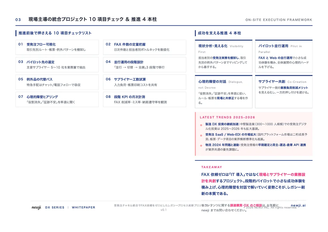
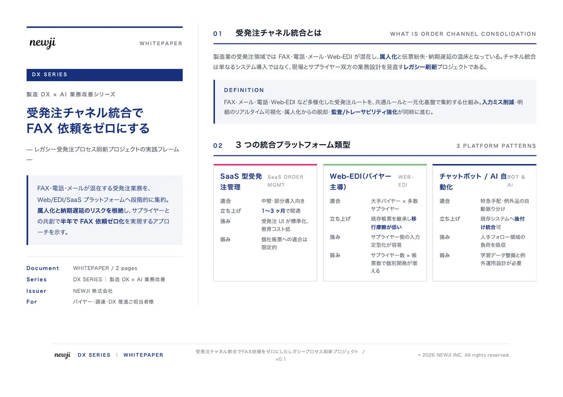
製造業の現場で使える実務資料(PDF)を無料でお届けします。"こんな資料が届きます" ↓ 下のボタンからどうぞ。
PRODUCT — 製造業向け 調達・受発注クラウド
この記事の課題、
newji で解決しませんか?
newji は、製造業の調達・受発注に特化したクラウド/AIエージェント。見積依頼・発注書作成・進捗管理・承認をひとつの画面に集約し、AIが比較と異常検知を担当。最後の「GO」だけ人が押す仕組みです。
- 見積〜発注〜納期を一元管理。催促・転記のムダをゼロに
- AIが相見積もり比較と異常検知。あなたは判断だけに集中
- 取引先は「招待」で完全無料。自社コストだけで取引先ごとデジタル化
※ 取引先から招待された企業様は完全無料でご利用いただけます
関連記事
-

PCB OEM: 調達購買で成功するための戦略とノウハウ
-

PCB OEMとデジタルトランスフォーメーション:未来の製造業をリードする方法
-

PCB OEMで製造業の未来をリードする:認知向上と販路拡大のための戦略
-
Transforming Modern Electronics: Unleashing the Potential of Silicon-on-Insulator (SOI) Technology for Enhanced Industry Recognition and Market Expansion
-
回路基板 (Printed Circuit Board, PCB)の設計と製造業での利用方法
-

回路基板 (Printed Circuit Board, PCB)の設計と調達業務での利用法
 調達購買アウトソーシング
 OEM/ODM 生産委託
 NEWJI DX
 受発注AIエージェント