

- お役立ち記事
- Fundamentals, applications, and high functionality of UV/EB curing technology
その単価は妥当か。
AI が根拠付きで分析。
相見積の比較も発注も進捗管理も、ひとつの画面に。

Fundamentals, applications, and high functionality of UV/EB curing technology

目次
Understanding UV/EB Curing Technology
Ultraviolet (UV) and Electron Beam (EB) curing technologies are advanced methods used in various industries for rapid curing or drying of coatings, inks, and adhesives.
Developed to replace conventional thermal drying methods, these technologies offer several advantages, including faster production speeds and reduced energy consumption.
Understanding the basics of UV/EB curing technology is essential for industries aiming to improve efficiency and product quality.
UV/EB curing involves the polymerization and cross-linking of monomers into polymers using electromagnetic radiation.
While the goal is the same—speeding up the curing process—each technology has distinct methods and applications.
UV Curing: How It Works
In UV curing, ultraviolet light is used to initiate a photochemical reaction.
This process requires special formulations of inks, coatings, or adhesives called UV-curable materials.
When UV light hits these materials, photoinitiators in the formulation absorb the light energy.
This energy converts them into reactive species, which then start the polymerization process.
The equipment necessary for UV curing includes UV lamps or LEDs, which emit wavelengths in the UV range.
Reflectors and cooling systems are often integrated to focus the radiation and manage equipment temperature.
Applications of UV Curing Technology
UV curing is popular in industries such as printing, electronics, automotive, and medical.
In printing, UV-curable inks offer high speed and vibrant, high-quality prints.
The electronics sector employs UV curing for the rapid processing of coatings on circuit boards.
Automotive industries use it for durable coatings, while the medical field utilizes it for producing safe and effective devices and equipment.
Additionally, UV coating is extensively used for surface treatments in woodworking and flooring, ensuring durability and aesthetic appeal.
How EB Curing Works
Electron Beam curing is a radiation-based method that uses high-energy electrons to cure materials.
Unlike UV curing, EB curing doesn’t require photoinitiators since the electrons themselves provide the necessary energy to drive the polymerization process.
The EB curing process involves directing a stream of electrons onto the material.
This energy breaks chemical bonds in the formulation, urging them to react and form polymers.
EB curing machines are composed of an electron gun, an accelerator, a chamber, and shielding to ensure safety from the radiation emitted.
Applications of EB Curing Technology
EB curing is particularly advantageous for industrial applications requiring depth curing and where darker or opaque surfaces are involved.
This technology sees extensive use in aerospace, packaging, and metal coating industries.
In packaging, to treat food-safe coatings on films and boxes, EB curing provides excellent results at high speeds.
In aerospace, the need for lightweight, durable materials is met through EB coatings that enhance performance.
Metal coating industries employ EB curing for its robust finishes and minimal impact on substrate integrity.
Advantages of UV/EB Curing Technologies
The appeal of UV and EB curing goes beyond rapid processing speeds.
One significant advantage is their lower energy consumption compared to traditional thermal drying, leading to lower operational costs and a reduced carbon footprint.
These technologies enable the use of more environmentally friendly formulations, often with low or no volatile organic compounds (VOCs), aligning with regulations and sustainability goals.
Both technologies also allow for continuous production lines due to their quick curing times, improving overall throughput and efficiency.
UV and EB curing systems require less floor space, as they don’t need the large ovens associated with thermal curing.
Comparing UV and EB Curing
While sharing many advantages, UV and EB curing have differences that suit varied applications.
UV curing is typically less costly than EB due to simpler equipment requirements.
However, UV curing can have limitations with depth penetration and sensitivity to substrate color and opacity.
On the other hand, EB curing, though more expensive initially, offers greater curing depth and is unaffected by viscosity or color.
This makes it apt for thicker materials and surfaces needing precise curing.
Challenges and Considerations
Despite the benefits, adopting UV/EB curing systems comes with challenges.
Initial investment costs can be high, especially for EB systems.
This requires careful evaluation of return on investment based on production needs and expected benefits.
Moreover, UV systems need precise control and maintenance to manage exposure and ensure even curing, while EB systems require stringent safety measures due to radiation exposure.
It is also crucial for businesses to assess the compatibility of their existing processes and materials with UV and EB technologies to make informed decisions.
The Future of UV/EB Curing Technologies
The demand for faster, efficient, and eco-friendly production processes is set to grow, expanding the use of UV/EB curing technologies.
Research and development are continually improving photoinitiators and formulations to overcome current limitations.
Furthermore, advancements in LED UV curing are making these systems more energy-efficient and versatile, opening new possibilities across diverse industries.
As technology progresses, industries will look to UV/EB curing for not only enhancing productivity but also for adhering to more stringent environmental regulations.
The adoption of these technologies represents a smart investment in sustainability and innovation, positioning businesses well for the future marketplace.
この記事の理解を深める
無料ホワイトペーパーをプレゼント
製造業の現場で使える実務資料(PDF)を無料でお届けします。"こんな資料が届きます" ↓ 下のボタンからどうぞ。
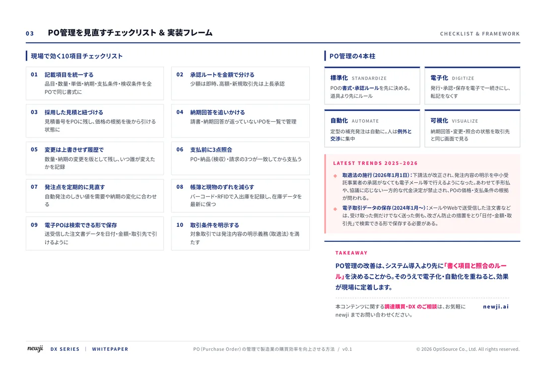
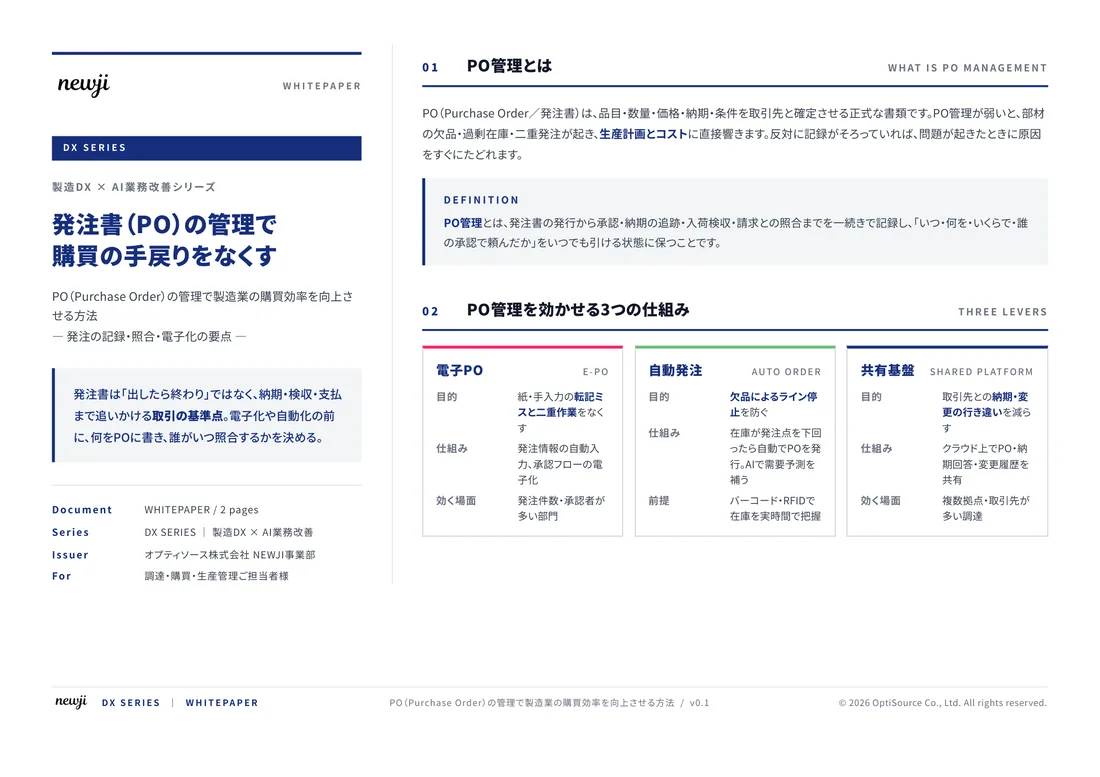
FREE DOCUMENT — サービス資料(PDF・無料)
製造業の見積・受発注クラウド
「Newji one」とは
Newji one は、製造業の調達・受発注に特化したクラウド/AIエージェント。見積依頼・発注書作成・進捗管理・承認をひとつの画面に集約し、AIが比較と異常検知を担当。最後の「GO」だけ人が押す仕組みです。
▶ 製造業の見積・受発注クラウド「Newji one」を、資料で見る(PDF・無料)
- 見積〜発注〜納期を一元管理。催促・転記のムダをゼロに
- AIが相見積もり比較と異常検知。あなたは判断だけに集中
- 取引先は「招待」で完全無料。自社コストだけで取引先ごとデジタル化
※ 取引先から招待された企業様は完全無料でご利用いただけます
関連記事
-

Transforming Modern Electronics: Unleashing the Potential of Silicon-on-Insulator (SOI) Technology for Enhanced Industry Recognition and Market Expansion
-

Energy Efficiency Improvement Strategies! Cost Reduction and Environmental Impact Reduction in Manufacturing
-
Energy-efficient production technology contributes to a sustainable future for manufacturing
-
Boosting Energy Efficiency and Reducing Costs in Manufacturing
-
Reducing Energy Efficiency and Environmental Impact The Path Paved by Digital
-
ゴム硬化(Rubber Curing)の技術と製造業での応用方法
 NEWJI総研
 OEM/ODM 生産委託
 AI/DX支援
 見積・発注クラウド Newji one
受発注が増えるほど、入力・確認・催促が重くなる。
受発注管理を“仕組み化“して、ミスと工数を削減しませんか。
見積・発注・納期まで一元管理できます。