

- お役立ち記事
- Fundamentals of silicon transistor technology, 3D packaging technology, and application to low power and high performance technology for CMOS devices

その単価は妥当か。
AI が根拠付きで分析。
相見積の比較も発注も進捗管理も、ひとつの画面に。

Fundamentals of silicon transistor technology, 3D packaging technology, and application to low power and high performance technology for CMOS devices

目次
Understanding Silicon Transistor Technology
Silicon transistors are at the heart of modern electronic devices.
These small yet powerful components are used to manage the flow of electrical current in circuits, functioning as switches or amplifiers.
Understanding the basics of silicon transistor technology is crucial for grasping how today’s electronics work and how they are evolving.
Silicon, a semiconducting material, is commonly used in the production of transistors due to its abundant availability and favorable electronic properties.
In a typical silicon transistor, small changes in voltage can control a large current flow.
This ability makes them ideal for use in computers, smartphones, and many other electronic gadgets.
The two primary types of transistors are Bipolar Junction Transistors (BJTs) and Field Effect Transistors (FETs).
While BJTs work by using a small current to control a larger one, FETs use electric fields to manage conductivity.
Complementary metal-oxide-semiconductor (CMOS) devices primarily use FETs because of their high efficiency and low power consumption.
Exploring 3D Packaging for Transistors
3D packaging technology is revolutionizing the way semiconductor devices are constructed and utilized.
This approach involves stacking multiple layers of integrated circuits (ICs) to create more compact and efficient components.
The layered configuration helps in reducing the overall footprint and improving performance metrics like speed and energy efficiency.
Unlike traditional 2D arrangements, 3D packaging allows for shorter interconnects between chips.
This results in faster data processing and communication within the system.
Moreover, the vertical integration offered by 3D packaging can support complex designs, facilitating the construction of advanced semiconductor architectures.
Companies invest in 3D packaging to overcome the limitations of scaling laws, such as Moore’s Law, which predicts the doubling of transistors in ICs about every two years.
3D packaging helps in maintaining this trend without the need of shrinking individual transistors further.
Advantages of 3D Packaging Technology
One of the primary advantages of 3D packaging is the increase in performance with reduced lag time.
It offers superior bandwidth and reduced latency compared to traditional methods.
This leads to quicker data transfer and processing, making devices faster and more responsive.
Energy efficiency is another crucial advantage.
3D packages reduce the distance that signals must travel, which decreases power consumption.
This is particularly beneficial for portable devices, where battery life is a limiting factor.
Improved thermal management is another strength of 3D packaging.
Heat dissipation is more efficient in 3D arrangements, preventing overheating and extending the device lifespan.
Applications of Transistors in Low Power and High Performance CMOS Devices
CMOS technology is widely used due to its low power consumption while providing high performance.
Silicon transistors play a key role in enabling these attributes, making CMOS the preferred choice for various applications.
Low Power Applications
In low power applications, such as mobile devices and IoT gadgets, being energy efficient is paramount.
CMOS technology excels here, allowing devices to operate longer on a single charge.
Power-saving features such as sleep modes and low-power states are enabled by the precise control transistors provide over current flow.
Wearable technology, such as smartwatches and fitness trackers, benefits enormously from low power transistors embedded in CMOS devices.
These products must sustain longer operational times while being small and lightweight.
High Performance Applications
For high performance, transistors in CMOS configurations offer quick switching capabilities and high-speed computation.
This is essential in processing-intensive applications such as gaming consoles, servers, and desktop processors.
The push for higher performance often demands that these devices handle more data at greater speeds, which is facilitated by advancements in silicon transistor technology.
These transistors utilize short channels, allowing electrons to move quickly from one terminal to another.
Fast processing rates reduce operating time and improve efficiency, making contemporary computing tools faster and more potent.
The Future of Silicon Transistors and Packaging Technologies
As the demand for more efficient and robust electronic components grows, the development of silicon transistors and their packaging technologies is likely to continue advancing.
Research and experimentation are ongoing to further shrink transistor sizes and enhance 3D packaging techniques.
These innovations promise to bring about even more powerful and energy-efficient electronic devices.
The integration of artificial intelligence and machine learning in designing transistors could lead to more intelligent automatic optimizations in these components.
This will result in an electronics ecosystem that self-adjusts for optimal performance.
Additionally, the movement toward sustainable technology guides the industry toward creating environmentally friendly solutions.
Higher efficiency and lower energy consumption align well with green technology goals, a factor that is becoming increasingly important with environmental concerns.
In conclusion, the intersection of silicon transistor technology, 3D packaging methods, and advances in low-power, high-performance CMOS devices marks a pivotal area of growth in the electronics industry.
These technologies not only push the boundaries of what is possible but also open new realms of opportunity for future applications.
この記事の理解を深める
無料ホワイトペーパーをプレゼント
製造業の現場で使える実務資料(PDF)を無料でお届けします。"こんな資料が届きます" ↓ 下のボタンからどうぞ。
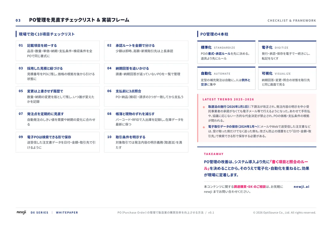
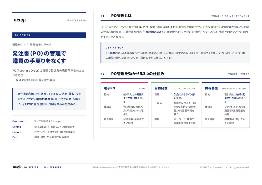
FREE DOCUMENT — サービス資料(PDF・無料)
製造業の見積・受発注クラウド
「Newji one」とは
Newji one は、製造業の調達・受発注に特化したクラウド/AIエージェント。見積依頼・発注書作成・進捗管理・承認をひとつの画面に集約し、AIが比較と異常検知を担当。最後の「GO」だけ人が押す仕組みです。
▶ 製造業の見積・受発注クラウド「Newji one」を、資料で見る(PDF・無料)
- 見積〜発注〜納期を一元管理。催促・転記のムダをゼロに
- AIが相見積もり比較と異常検知。あなたは判断だけに集中
- 取引先は「招待」で完全無料。自社コストだけで取引先ごとデジタル化
※ 取引先から招待された企業様は完全無料でご利用いただけます
関連記事
-

Transforming Modern Electronics: Unleashing the Potential of Silicon-on-Insulator (SOI) Technology for Enhanced Industry Recognition and Market Expansion
-

Silicon Carbideを活用した次世代製造プロセスの最適化方法
-

Energy Efficiency Improvement Strategies! Cost Reduction and Environmental Impact Reduction in Manufacturing
-
Energy-efficient production technology contributes to a sustainable future for manufacturing
-
半導体にはどのような電子部品が搭載されているのか?
-

絶縁ゲートバイポーラトランジスタ(IGBT)とMOSFETの違い
 NEWJI総研
 OEM/ODM 生産委託
 AI/DX支援
 見積・発注クラウド Newji one
受発注が増えるほど、入力・確認・催促が重くなる。
受発注管理を“仕組み化“して、ミスと工数を削減しませんか。
見積・発注・納期まで一元管理できます。