

- お役立ち記事
- Ideal for complex wiring boards! Prototype via holes with μm precision using UV laser drilling

スタートアップから大手まで。
調達・受発注をAIで標準化。
相見積比較も進捗管理もAIが下支え。取引先は招待で完全無料。

Ideal for complex wiring boards! Prototype via holes with μm precision using UV laser drilling

目次
Understanding Via Holes in PCB Manufacturing
In the world of electronic circuit boards, precision is crucial.
When it comes to ensuring smooth electrical connections between different layers of a PCB (Printed Circuit Board), via holes play an essential role.
These small yet significant components act as conduits, allowing signals and electrical current to travel across the multiple layers of a board.
Creating these tiny via holes requires meticulous processes, especially as modern requirements demand even smaller and more precise connections.
This is where advancements in technology, such as UV laser drilling, come into play.
Why UV Laser Drilling Is Essential
With the increased demand for miniaturization in electronics, manufacturers are challenged to enhance the precision and capability of their PCB production methods.
Traditional mechanical drilling methods often fall short when it comes to producing the micro-sized via holes required.
Enter UV laser drilling, a method that enables manufacturers to achieve micrometer-level precision in drilling operations.
UV laser drilling offers several advantages.
Firstly, it allows for the creation of extremely small via holes without causing damage to the surrounding materials on the board.
This precision is crucial, as even slight damage or misalignment can lead to connectivity issues or product failure.
Secondly, the process is non-contact, meaning there is no physical wear and tear on the tools used.
This enhances the longevity of the equipment and results in cost savings over time.
Finally, the UV laser method is versatile and can adapt to various materials typically used in PCB manufacturing, offering even more flexibility and reliability in production.
The Mechanics Behind UV Laser Drilling
UV lasers use a focused beam of ultraviolet light to ablate material from the PCB.
This method allows for precise control over the drilling process, minimizing material wastage and ensuring consistent hole size and placement.
One of the main advantages of UV lasers is their ability to operate at high speeds, significantly reducing the time needed to complete drilling operations compared to mechanical methods.
The laser can rapidly create thousands of precise via holes, which is essential for the production of dense and complex circuit boards.
Applications of UV Laser Drilling in PCB Manufacturing
UV laser drilling is particularly beneficial in areas where advanced and compact electronic devices are being developed.
For instance, in the consumer electronics industry, the demand for smaller and more efficient smartphones, tablets, and wearables has pushed manufacturers to adopt such precision drilling techniques.
Another area where UV laser drilling excels is in the automotive industry.
With the rise of electric vehicles and autonomous driving technologies, the need for high-performance, reliably connected PCBs has increased.
UV laser drilling ensures that these complex boards can meet the stringent demands of the automotive sector.
Moreover, in aerospace and medical device manufacturing, where reliability and precision are non-negotiable, UV laser drilling ensures that the circuit boards used are of the highest quality.
Taking Prototypes to the Next Level
Before any product hits mass production, prototypes play an essential role in fine-tuning and testing designs.
UV laser drilling is ideal for prototyping purposes due to its precision and adaptability, allowing engineers to experiment with various designs and configurations without committing to full-scale production runs.
The precision of UV laser drilling ensures that the prototype boards are as close as possible to their final iteration, reducing the need for adjustments and modifications later in the production process.
This increases efficiency and speeds up the time to market.
Environmental Considerations
As industries shift towards greener and more sustainable practices, the environmental impact of manufacturing processes is under scrutiny.
UV laser drilling contributes positively in this regard, as it reduces material waste and energy consumption compared to traditional drilling methods.
Additionally, the process generates fewer residues and by-products, making it a cleaner option that aligns with the growing emphasis on environmental responsibility in manufacturing.
Conclusion
In summary, as the demand for smaller, more complex, and reliable PCBs continues to grow, UV laser drilling emerges as an indispensable tool for manufacturers.
Its ability to produce via holes with μm precision ensures the integrity and performance of the final product.
By adopting this cutting-edge technology, manufacturers can not only improve efficiency and reduce costs but also contribute to more sustainable production practices.
This blend of precision, speed, and environmental benefits makes UV laser drilling a clear choice for any production facility aiming to stay competitive in the ever-evolving electronics industry.
この記事の理解を深める
無料ホワイトペーパーをプレゼント
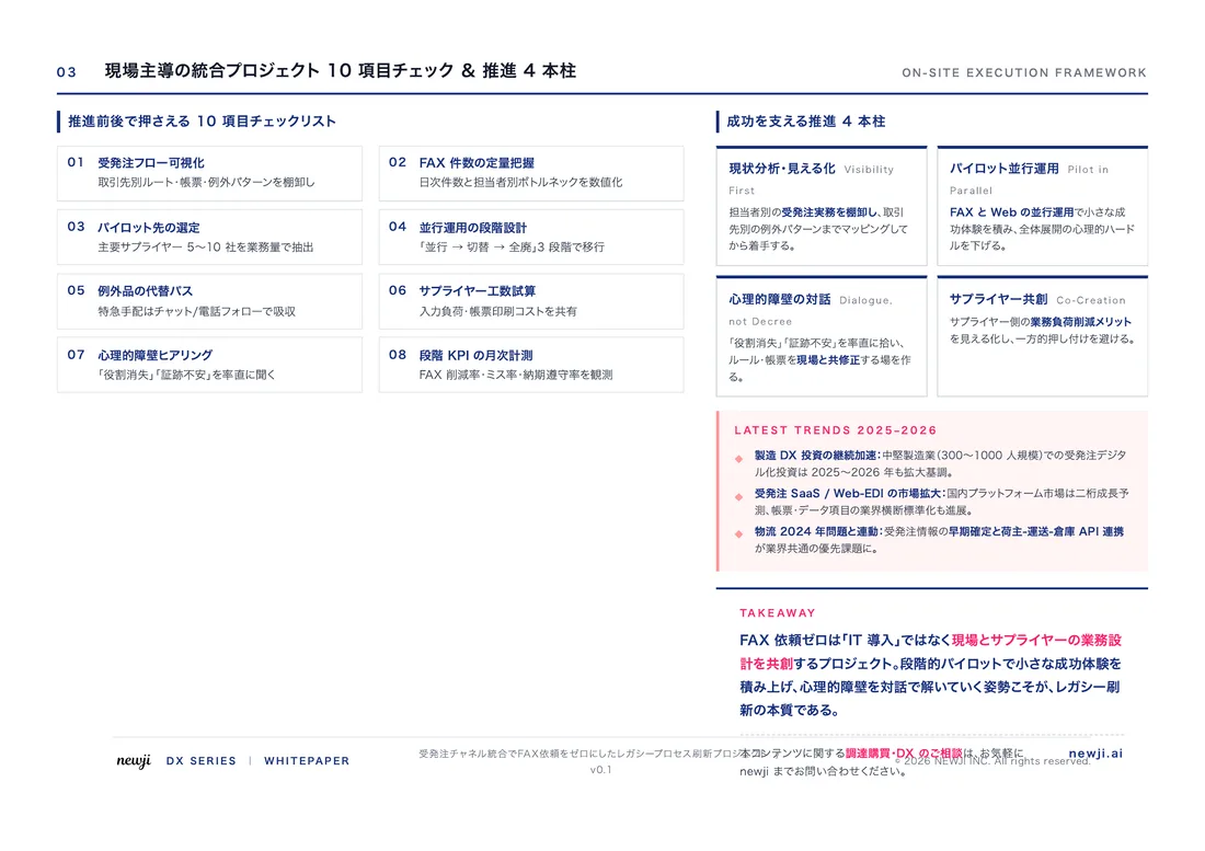
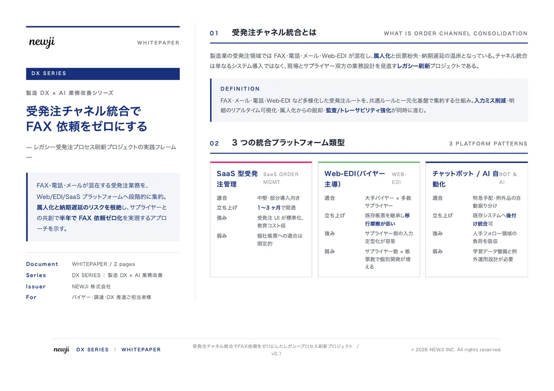
製造業の現場で使える実務資料(PDF)を無料でお届けします。"こんな資料が届きます" ↓ 下のボタンからどうぞ。
PRODUCT — 製造業向け 調達・受発注クラウド
この記事の課題、
newji で解決しませんか?
newji は、製造業の調達・受発注に特化したクラウド/AIエージェント。見積依頼・発注書作成・進捗管理・承認をひとつの画面に集約し、AIが比較と異常検知を担当。最後の「GO」だけ人が押す仕組みです。
- 見積〜発注〜納期を一元管理。催促・転記のムダをゼロに
- AIが相見積もり比較と異常検知。あなたは判断だけに集中
- 取引先は「招待」で完全無料。自社コストだけで取引先ごとデジタル化
※ 取引先から招待された企業様は完全無料でご利用いただけます





 調達購買アウトソーシング
 OEM/ODM 生産委託
 NEWJI DX
 受発注AIエージェント