

- お役立ち記事
- Latest technological trends and applications of high thermal conductivity photosensitive materials

Latest technological trends and applications of high thermal conductivity photosensitive materials

目次
Understanding High Thermal Conductivity Photosensitive Materials
High thermal conductivity photosensitive materials are at the forefront of technological advancement, offering exciting applications across a spectrum of industries.
These materials are becoming increasingly significant due to their ability to manage heat effectively while maintaining sensitivity to light.
Photosensitive materials have been used for years in various applications, from photography to lithography.
However, the recent development of photosensitive materials with high thermal conductivity has broadened their potential uses significantly.
The enhanced thermal management these materials provide helps in reducing heat buildup, which is a crucial issue in electronic and photonic devices.
Managing this heat effectively can lead to increased efficiency, performance, and lifespan of these devices.
Technological Trends in Photosensitive Materials
Several technological trends are driving the development of high thermal conductivity photosensitive materials.
Researchers are continuously working to improve the thermal properties of these materials without compromising their photosensitivity.
For example, there is an ongoing effort to integrate carbon reinforcements into photosensitive materials.
Carbon, particularly in forms like nanotubes and graphene, is renowned for its excellent thermal conductivity.
Incorporating these elements can dramatically enhance the material’s ability to transfer heat.
Nanotechnology is another key trend influencing advancements in this field.
By developing materials at the nanoscale, researchers can alter and enhance the thermal conductivity properties while still maintaining the necessary sensitivity to light.
This manipulation at the molecular level promises materials that are not only effective but also highly efficient.
Moreover, the trend towards flexible electronics is creating demand for photosensitive materials that can be bent and shaped without losing functionality.
High thermal conductivity materials are crucial here, as they prevent heat from becoming concentrated in one area, which is often a risk with flexible devices.
Applications of High Thermal Conductivity Photosensitive Materials
The applications of these advanced materials span across various fields, with significant potential in electronics, energy systems, and even medical devices.
Electronics and Photonics
In the electronics industry, high thermal conductivity photosensitive materials are extremely valuable.
They are used in the development of smaller, more efficient devices, capable of handling greater power outputs without overheating.
These materials can assist in the efficient dissipation of heat in integrated circuits and light-emitting diodes (LEDs).
By improving the heat management in these components, electronic devices can achieve higher performance and reliability while being more compact.
Energy Systems
Another area where these materials are finding application is in energy systems, particularly in solar panels.
Photosensitive materials that also possess high thermal conductivity can enhance the performance of photovoltaic cells.
They achieve this by both maximizing the absorption of light and minimizing thermal losses.
As the world moves towards more sustainable energy solutions, the ability to improve the efficiency of solar power technology is critical.
High thermal conductivity photosensitive materials are thus instrumental in driving this change.
Medical Devices
In the medical field, precision is key.
The integration of high thermal conductivity materials in medical devices ensures that heat generated from electronic components does not interfere with device performance or patient safety.
Wearable devices, which often make use of photosensitive materials for monitoring purposes, greatly benefit from improved thermal management.
This development enhances user comfort and device reliability, leading to more accurate health monitoring and diagnostics.
Challenges and Future Prospects
Despite the exciting potential of high thermal conductivity photosensitive materials, there are still challenges to be addressed.
Material Compatibility
Material compatibility remains a hurdle, as integrating high thermal conductivity features often requires new bonding methods that maintain both electrical integrity and thermal efficiency.
Ongoing research into hybrid materials is hopeful, however, as it suggests a future where seamless integration without loss of performance is possible.
Cost and Scalability
Price remains another barrier.
The production of advanced materials with both high thermal conductivity and photosensitivity can be expensive.
As research progresses, economies of scale and technological improvements are expected to reduce costs, making these materials accessible for wider commercial use.
The Road Ahead
Looking forward, it is clear that high thermal conductivity photosensitive materials will play an increasingly prominent role in numerous sectors.
As technology continues to advance, these materials will keep evolving to meet new demands, encompassing everything from the next generation of electric cars to the tiniest medical sensors.
For companies and industries seeking to push the boundaries of innovation, investing in this technology today will likely yield significant benefits tomorrow.
Maintaining attention on research, development, and the optimization of these materials is essential to fully harness their potential and address ongoing challenges.
This will pave the way for groundbreaking applications that not only enhance existing technology but also create entirely new fields of innovation.
この記事の理解を深める
無料ホワイトペーパーをプレゼント
製造業の現場で使える実務資料(PDF)を無料でお届けします。"こんな資料が届きます" ↓ 下のボタンからどうぞ。
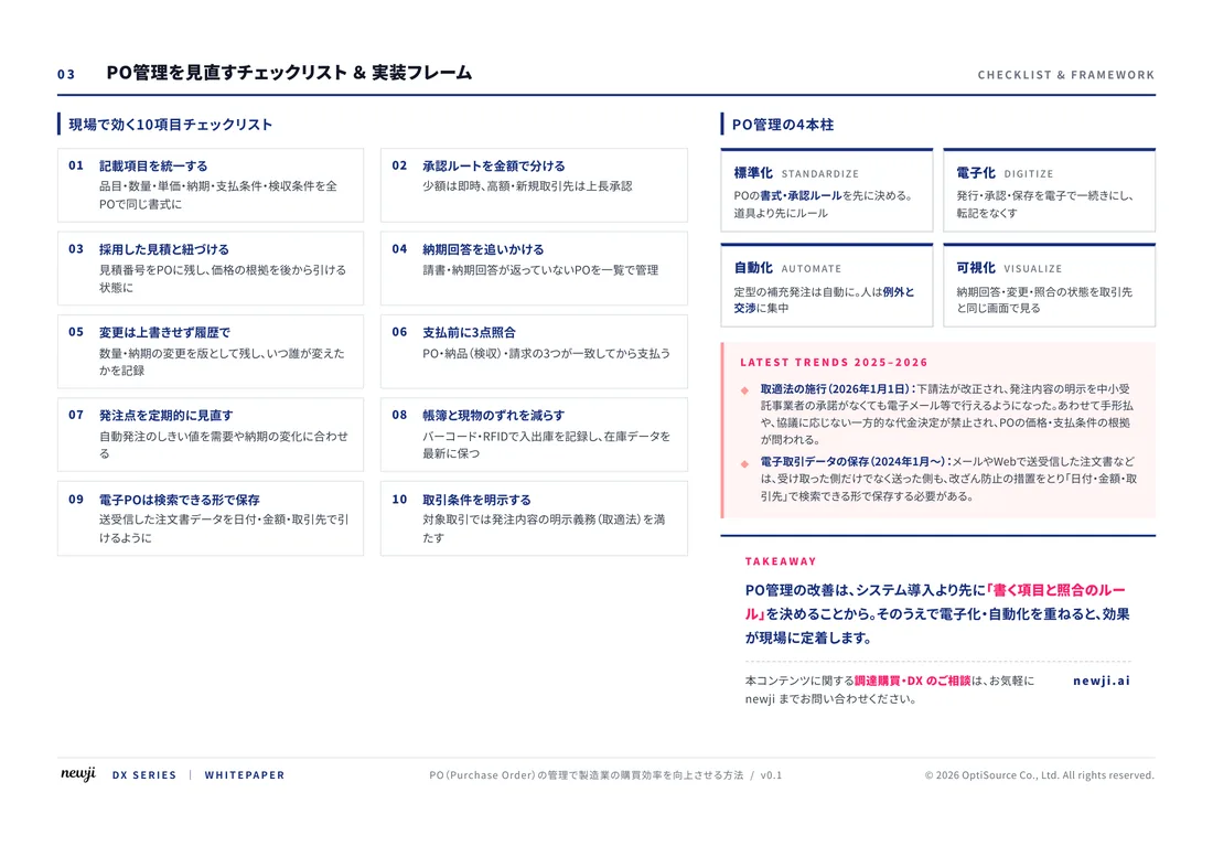
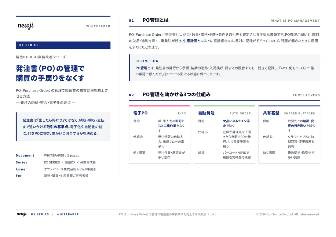
FREE DOCUMENT — サービス資料(PDF・無料)
製造業の見積・受発注クラウド
「Newji one」とは
Newji one は、製造業の調達・受発注に特化したクラウド/AIエージェント。見積依頼・発注書作成・進捗管理・承認をひとつの画面に集約し、AIが比較と異常検知を担当。最後の「GO」だけ人が押す仕組みです。
▶ 製造業の見積・受発注クラウド「Newji one」を、資料で見る(PDF・無料)
- 見積〜発注〜納期を一元管理。催促・転記のムダをゼロに
- AIが相見積もり比較と異常検知。あなたは判断だけに集中
- 取引先は「招待」で完全無料。自社コストだけで取引先ごとデジタル化
※ 取引先から招待された企業様は完全無料でご利用いただけます
関連記事
-

Transforming Modern Electronics: Unleashing the Potential of Silicon-on-Insulator (SOI) Technology for Enhanced Industry Recognition and Market Expansion
-

Energy Efficiency Improvement Strategies! Cost Reduction and Environmental Impact Reduction in Manufacturing
-
Energy-efficient production technology contributes to a sustainable future for manufacturing
-

熱伝導性 (Thermal Conductivity) の評価と製造業での利用方法
-
Boosting Energy Efficiency and Reducing Costs in Manufacturing
-
電気伝導性 (Electrical Conductivity) の評価と製造業での利用方法
 NEWJI総研
 OEM/ODM 生産委託
 AI/DX支援
 見積・発注クラウド Newji one
受発注が増えるほど、入力・確認・催促が重くなる。
受発注管理を“仕組み化“して、ミスと工数を削減しませんか。
見積・発注・納期まで一元管理できます。