

- お役立ち記事
- Metasurface and Metalens Technology: Fabrication and Industrial Applications

スタートアップから大手まで。
調達・受発注をAIで標準化。
相見積比較も進捗管理もAIが下支え。取引先は招待で完全無料。

Metasurface and Metalens Technology: Fabrication and Industrial Applications

目次
Understanding Metasurfaces and Metalenses
Metasurfaces and metalenses represent a groundbreaking advancement in the field of optics and photonics, offering new possibilities for controlling light with unprecedented precision.
These technologies have emerged as key players in various industrial applications, thanks to their unique properties and the potential they offer for innovation.
A metasurface is a two-dimensional material engineered to have specific optical properties.
It is composed of an array of nanostructures, each smaller than the wavelength of the light it interacts with.
These nanostructures manipulate light in ways that traditional optics cannot, enabling functionalities like bending, focusing, or scattering light with remarkable accuracy.
Metalenses, on the other hand, are special types of lenses made using metasurfaces.
They are capable of focusing light with minimal aberrations and at scales much smaller than conventional lenses.
This opens up new possibilities for compact and efficient optical systems in various industries, such as imaging, communications, and even medicine.
Fabrication of Metasurfaces and Metalenses
The fabrication of metasurfaces and metalenses involves advanced nanofabrication techniques that allow for the precise control of nano-sized structures.
These technologies rely heavily on the use of materials like metals, semiconductors, and dielectrics, which are manipulated on a nano-scale to achieve desired optical properties.
The process begins with the design of the metasurface structure, where computational models predict how these tiny elements will interact with light.
This design process is crucial as the arrangement and size of the nanostructures determine the functionality of the metasurface.
Next, the fabrication process typically involves lithography techniques, such as electron beam lithography or photolithography.
These methods allow for the precise patterning of nanostructures onto a substrate.
High-resolution lithography is essential because any deviation from the design can result in a significant loss of performance.
Once the nanostructures are patterned, they undergo processes like etching or deposition to form the final metasurface.
The choice of materials and precise control of the fabrication conditions are critical to ensure the metasurface performs as intended.
Challenges in Fabrication
Despite their potential, the fabrication of metasurfaces and metalenses poses several challenges.
One of the main difficulties is maintaining uniformity and precision across large areas, which is crucial for practical applications.
In addition, the fabrication process can be costly and time-consuming, which may limit large-scale production.
Another challenge is the integration of metasurfaces into existing systems.
Compatibility with current technologies and ensuring reliable performance are essential considerations during the design and fabrication phases.
Industrial Applications
The unique properties of metasurfaces and metalenses have led to their adoption in various industrial applications.
Their ability to control light with high precision makes them attractive for a wide range of uses.
Imaging Systems
In the field of imaging systems, metalenses offer several advantages over traditional lenses.
They enable the creation of thinner, lighter, and more compact optical systems, which are particularly beneficial for mobile devices like smartphones and cameras.
Moreover, metalenses can improve image quality by reducing aberrations, resulting in clearer and sharper images.
Communications
Metasurfaces also play a significant role in the telecommunications industry.
They are used to design antennas with enhanced performance, facilitating better signal reception and transmission.
The ability of metasurfaces to control electromagnetic waves makes them ideal for applications in high-frequency communication systems, such as 5G networks.
Medical Devices
In the medical field, metalenses are revolutionizing diagnostic and imaging tools.
Their compact size and lightweight nature make them suitable for integration into endoscopic and surgical instruments, where space and weight are critical constraints.
This can lead to more precise and less invasive procedures.
Augmented and Virtual Reality
Metasurfaces are also making significant strides in the world of augmented and virtual reality (AR/VR).
They enable the development of high-resolution headsets that are both lightweight and comfortable, enhancing the user experience.
By improving the optical performance of AR/VR devices, metasurfaces can help achieve more realistic and immersive environments.
Future Prospects
The future prospects of metasurface and metalens technology are promising, with ongoing research and development activities aiming to overcome current limitations.
Innovations in fabrication techniques are expected to reduce costs and improve scalability, making these technologies more accessible for widespread use.
Researchers are also exploring new materials and design strategies to enhance the performance of metasurfaces and metalenses.
By pushing the boundaries of what is possible, these advancements could lead to even more innovative applications, from quantum computing to advanced sensing systems.
Furthermore, as our understanding of light-matter interactions deepens, metasurfaces could unlock new functionalities that are currently unimaginable.
The integration of metasurfaces with other emerging technologies, such as artificial intelligence and machine learning, could open up exciting new avenues for research and application.
In conclusion, metasurface and metalens technologies represent a significant leap forward in the manipulation of light.
Their unique properties and potential applications make them a cornerstone for innovation across a variety of fields.
As research continues to evolve, the possibilities for these technologies appear boundless, promising a future where they become integral components of everyday life.
この記事の理解を深める
無料ホワイトペーパーをプレゼント
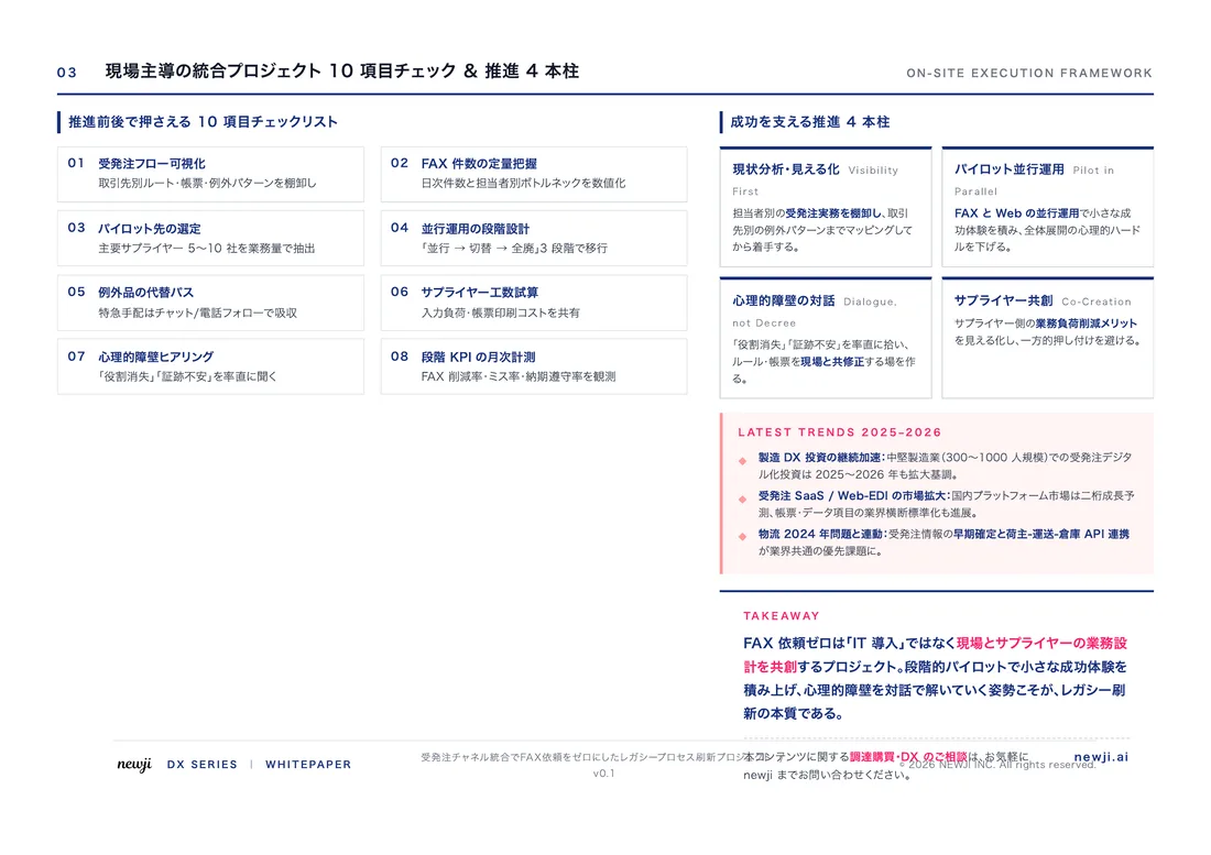
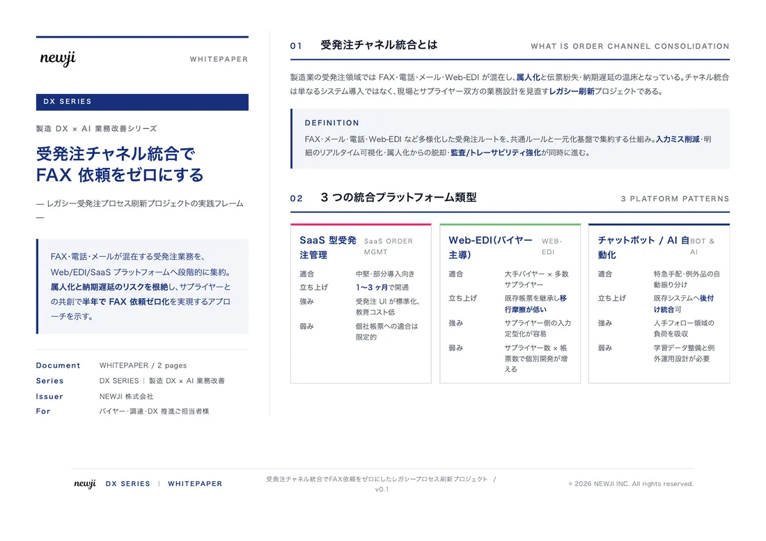
製造業の現場で使える実務資料(PDF)を無料でお届けします。"こんな資料が届きます" ↓ 下のボタンからどうぞ。
PRODUCT — 製造業向け 調達・受発注クラウド
この記事の課題、
newji で解決しませんか?
newji は、製造業の調達・受発注に特化したクラウド/AIエージェント。見積依頼・発注書作成・進捗管理・承認をひとつの画面に集約し、AIが比較と異常検知を担当。最後の「GO」だけ人が押す仕組みです。
- 見積〜発注〜納期を一元管理。催促・転記のムダをゼロに
- AIが相見積もり比較と異常検知。あなたは判断だけに集中
- 取引先は「招待」で完全無料。自社コストだけで取引先ごとデジタル化
※ 取引先から招待された企業様は完全無料でご利用いただけます
関連記事
-

GPON(Gigabit Passive Optical Network)の導入で工場のネットワークを強化する
-

Transforming Modern Electronics: Unleashing the Potential of Silicon-on-Insulator (SOI) Technology for Enhanced Industry Recognition and Market Expansion
-
EPON(Ethernet Passive Optical Network)を導入して工場のネットワークを強化する方法
-

「製造業におけるPON (Passive Optical Network) の導入が営業力を変革する理由」
-
EPON(Ethernet Passive Optical Network)を導入して工場のネットワークを強化する方法
-

製造業DX革新:PON技術がもたらす産業ネットワークの新時代

 調達購買アウトソーシング
 OEM/ODM 生産委託
 NEWJI DX
 受発注AIエージェント