

- お役立ち記事
- For new employees in the R&D department! Fundamentals of nanotechnology and practice of innovative material development

スタートアップから大手まで。
調達・受発注をAIで標準化。
相見積比較も進捗管理もAIが下支え。取引先は招待で完全無料。

For new employees in the R&D department! Fundamentals of nanotechnology and practice of innovative material development

目次
Understanding Nanotechnology
Nanotechnology is a fascinating field that is revolutionizing industries by offering new possibilities in material development.
It involves manipulating matter on an atomic and molecular scale, typically below 100 nanometers.
To grasp its sheer potential, imagine a single strand of human hair, which is around 80,000 nanometers wide.
Nanotechnology takes us several thousands of times smaller, where atoms and molecules can be meticulously arranged.
The ability to control materials on this level opens doors to innovation, especially in research and development (R&D) sectors.
Basic Concepts in Nanotechnology
To navigate the world of nanotechnology, it’s important to understand its core principles.
The primary idea is to harness unique phenomena exhibited at the nanoscale.
At this level, materials often display different electrical, chemical, and mechanical properties compared to their macroscopic counterparts.
These changes are due to the increased surface area-to-volume ratio and quantum effects that dominate at the nanoscale.
This leads to innovations like stronger yet lighter materials, enhanced catalysts, and improved electrical conductors.
Additionally, some nanoparticles can transition between materials state like solids, liquids, and gases without changing temperature, offering new processing methods.
Applications of Nanotechnology in Material Development
Nanotechnology is used across multiple industries to develop innovative materials that are stronger, lighter, and more efficient.
In the field of electronics, nanoscale transistors lead to faster and more powerful computers.
Medical applications include drug delivery systems where nanoparticles target specific cells or tissues, minimizing side effects and improving treatment efficacy.
Nanomaterials can create water-repellent, stain-resistant, and antimicrobial surfaces, useful in both consumer and industrial products.
In energy, nanotechnology improves the efficiency of solar cells and batteries.
Finally, nanocomposites enhance vehicle performance through weight reduction, leading to better fuel efficiency and reduced emissions.
Steps in Innovative Material Development
As a new employee in the R&D department, developing innovative materials using nanotechnology requires a structured approach.
The process typically involves several key steps that ensure successful experimentation and implementation.
Step 1: Define Objectives and Requirements
Before beginning any development, clearly define the objectives.
Understand what specific properties your material must exhibit and where it will be applied.
Will the focus be on enhancing strength, conductivity, or biocompatibility?
Outline requirements to guide your research and align project goals.
Detailed planning at this stage is crucial, as it sets the foundation for your project plan.
Step 2: Research and Design
Engage in comprehensive research to understand the fundamentals and recent advancements in your field of interest.
Study materials known to exhibit desired traits at the nanoscale.
Based on this information, design a theoretical model or structure for your material.
Consider different methods of synthesis or fabrication that are feasible for achieving the nanoscale structure.
Simulations and computer modeling can be highly beneficial at this stage, predicting behavior before physical testing.
Step 3: Synthesis and Fabrication
Once your design is clarified, move to the experimental phase, where materials are synthesized and fabricated.
Techniques such as chemical vapor deposition, molecular beam epitaxy, and sol-gel processes are common in laboratory settings.
Precise control is necessary to ensure the desired nanoscale properties are achieved.
This may require specialized equipment capable of altering conditions like temperature, pressure, and chemical composition.
Step 4: Characterization
After fabrication, thoroughly characterize the developed material to verify if it meets your design specifications.
Apply various analytical techniques such as electron microscopy, X-ray diffraction, and spectroscopic methods.
These tools help visualize the structure and surface architecture, providing insight into the material’s nanoscale properties.
Characterization also involves testing mechanical, electrical, and thermal properties in the lab.
Effective comparison between expected and actual performance lays the groundwork for the next steps.
Step 5: Testing and Iteration
Materials often require iteration for optimization.
Conduct practical testing under simulated conditions relevant to real-world applications.
Analyze performance against established benchmarks and refine your material by adjusting parameters or refining synthesis methods.
Iteration is vital for overcoming unforeseen challenges, ensuring resilience and reliability.
Step 6: Practical Application and Evaluation
Upon reaching an optimized state, integrate your new material into a prototype or product for practical application.
Evaluate its performance in the intended environment, gathering data and feedback from stakeholders.
If successful, prepare documentation for patents or intellectual property rights, protecting your innovative work.
These evaluations guide scaling up production and commercialization strategies.
Preparing for Future Innovations
Staying adaptable and continuously learning is key to success in nanotechnology-based material development.
Engage in professional education through courses, workshops, and conferences to stay updated with the latest advancements.
Collaborate with scientists and engineers across disciplines, enriching your perspective and fostering innovative ideas.
Tracking market trends helps anticipate future needs, guiding your research towards impactful solutions.
Through dedication and teamwork, fresh ideas will continue to emerge, pushing the boundaries of what’s possible with nanotechnology.
この記事の理解を深める
無料ホワイトペーパーをプレゼント
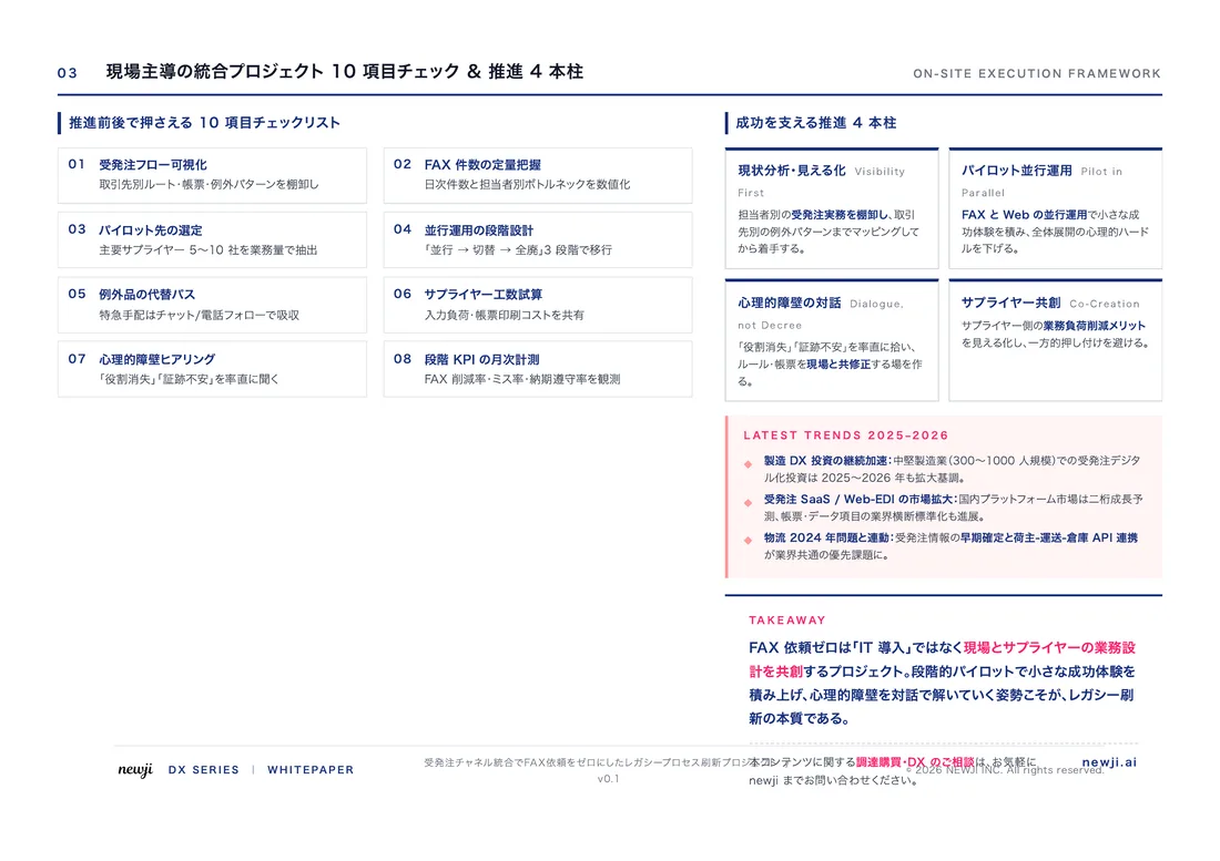
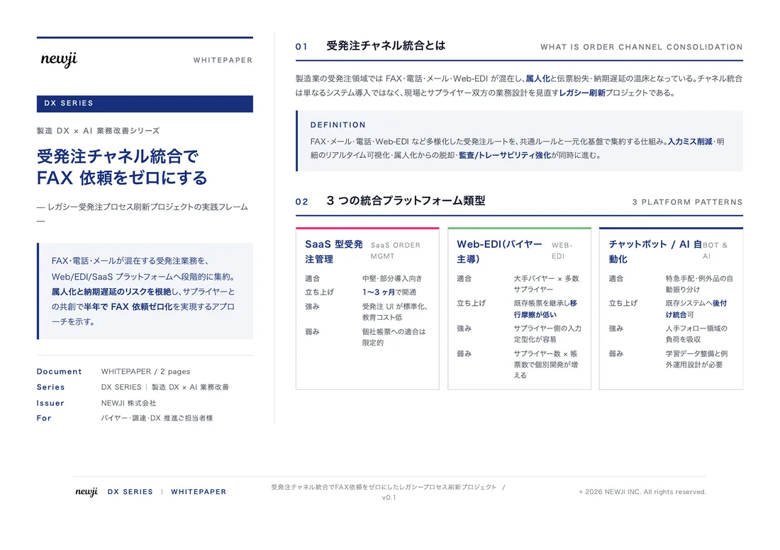
製造業の現場で使える実務資料(PDF)を無料でお届けします。"こんな資料が届きます" ↓ 下のボタンからどうぞ。
PRODUCT — 製造業向け 調達・受発注クラウド
この記事の課題、
newji で解決しませんか?
newji は、製造業の調達・受発注に特化したクラウド/AIエージェント。見積依頼・発注書作成・進捗管理・承認をひとつの画面に集約し、AIが比較と異常検知を担当。最後の「GO」だけ人が押す仕組みです。
- 見積〜発注〜納期を一元管理。催促・転記のムダをゼロに
- AIが相見積もり比較と異常検知。あなたは判断だけに集中
- 取引先は「招待」で完全無料。自社コストだけで取引先ごとデジタル化
※ 取引先から招待された企業様は完全無料でご利用いただけます
関連記事
-

Transforming Modern Electronics: Unleashing the Potential of Silicon-on-Insulator (SOI) Technology for Enhanced Industry Recognition and Market Expansion
-

ナノテクノロジー(Nanotechnology)の利点と製造業での応用方法
-

Evolution of 3D Printing Technology Revolutionizing Manufacturing
-

Saving Time and Money in Manufacturing Leads to Efficient Material Handling
-
Innovative Aerodynamic Skin Material: Revolutionizing Performance and Efficiency in Aerospace Manufacturing
-

Harnessing the Potential of Nano-Engineered Rubber: A Procurement Leader’s Guide to Innovative Material Sourcing

 調達購買アウトソーシング
 OEM/ODM 生産委託
 NEWJI DX
 受発注AIエージェント