

- お役立ち記事
- High-precision laser annealing techniques that process engineers in the semiconductor manufacturing industry should know

スタートアップから大手まで。
調達・受発注をAIで標準化。
相見積比較も進捗管理もAIが下支え。取引先は招待で完全無料。

High-precision laser annealing techniques that process engineers in the semiconductor manufacturing industry should know

目次
Introduction to Laser Annealing
Laser annealing is a sophisticated process that plays a crucial role in the semiconductor manufacturing industry.
With the continuous need for miniaturization and increased performance in electronic devices, laser annealing has become an indispensable technique.
Essentially, it involves using laser light to heat materials quickly and precisely, thereby altering their properties and enhancing their performance.
This method is particularly valuable in addressing the challenges of modern semiconductor fabrication, such as achieving high precision and maintaining efficiency.
Why Laser Annealing is Important
The significance of laser annealing lies in its precision and effectiveness.
It allows semiconductor manufacturers to selectively heat specific areas of a material without affecting the surrounding regions.
This precision is paramount in semiconductor manufacturing, where even a slight deviation can impact the functionality of an electronic device.
Moreover, laser annealing can be performed at room temperature, which reduces the risk of thermal damage to the substrate.
This makes it a preferred technique over traditional thermal annealing, especially for delicate wafer materials.
Types of Laser Annealing Techniques
There are several laser annealing techniques, each suited to different manufacturing requirements.
Understanding these techniques helps process engineers choose the right method for their specific applications.
Pulsed Laser Annealing (PLA)
Pulsed Laser Annealing is a method where short laser pulses are used to heat the material’s surface rapidly.
This type is ideal for processes requiring high localized temperatures on the wafer surface.
PLA is commonly used in processes involving dopant activation where short, intense bursts of light are needed to activate the dopants without affecting the wafer’s bulk.
Continuous Wave Laser Annealing (CWLA)
In Continuous Wave Laser Annealing, a continuous laser beam is applied to the material.
This technique is suitable for applications requiring uniform heating over a larger area.
CWLA is often preferred for processes that necessitate steady and controlled thermal exposure to achieve homogenous material modifications.
Laser-Induced Forward Transfer (LIFT)
Laser-Induced Forward Transfer is a unique technique whereby a laser beam is used to transfer material from a donor substrate to a receiver substrate.
This method is used in situations where material needs to be deposited with high precision.
LIFT is particularly valuable in creating intricate patterns or when working with sensitive materials that are prone to thermal damage.
Applications of Laser Annealing in Semiconductor Manufacturing
Laser annealing has a wide range of applications in the semiconductor manufacturing industry.
Dopant Activation
One of the primary uses of laser annealing is in dopant activation.
Dopants are introduced into semiconductor materials to modify their electrical properties.
Laser annealing is used to activate these dopants by using carefully controlled thermal energy, ensuring they achieve the desired electrical characteristics without causing damage to the wafer.
Thin Film Transistor (TFT) Processing
Laser annealing is critical in the production of Thin Film Transistors, which are essential components in display technologies like LCDs and OLEDs.
Using laser annealing, these transistors can be processed to improve their electrical performance, offering clearer displays and better energy efficiency.
Advanced Packaging Techniques
In advanced semiconductor packaging, laser annealing is used to enhance the interconnections within the devices.
It allows for the creation of more reliable and efficient connections between microelectronic components, leading to smaller, faster, and more powerful devices.
Challenges and Considerations
While laser annealing offers a host of advantages, it also presents certain challenges that engineers must consider.
Precision Alignment
Achieving precision alignment is crucial in laser annealing.
Even minor misalignments can lead to defects in the semiconductor devices.
As such, sophisticated equipment and careful calibration are needed to ensure that laser energy is applied accurately.
Material Compatibility
Not all materials respond to laser annealing in the same way.
Different materials have different thermal properties, requiring engineers to tailor the laser annealing process specific to the material being treated.
Finding the optimal balance between laser power, exposure time, and wavelength is vital to avoid undesirable effects such as warping or melting.
Future Trends in Laser Annealing
The future of laser annealing in semiconductor manufacturing looks promising, with ongoing advancements and new trends emerging.
Integration with AI and Automation
As industries move towards automation, integrating laser annealing processes with AI systems is becoming more common.
AI can help optimize the laser parameters in real-time, improving precision while reducing material waste and production time.
Development of New Materials
Ongoing research in materials science is likely to produce new materials with unique properties that can be processed using laser annealing.
These developments will enable manufacturers to create more efficient semiconductor devices, catering to the growing demand for high-performance electronics.
Conclusion
High-precision laser annealing techniques are indispensable in the modern semiconductor manufacturing industry.
They offer the precision, speed, and efficiency needed to produce the next generation of electronic devices.
As technology advances, these techniques will continue to evolve, offering even greater capabilities and opportunities for innovation in semiconductor fabrication.
Understanding and mastering these techniques is crucial for process engineers aiming to excel in the competitive field of semiconductor manufacturing.
この記事の理解を深める
無料ホワイトペーパーをプレゼント
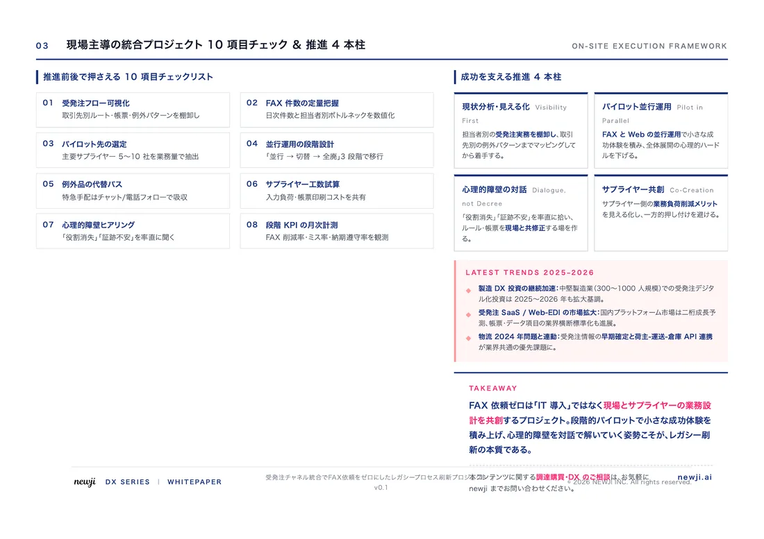
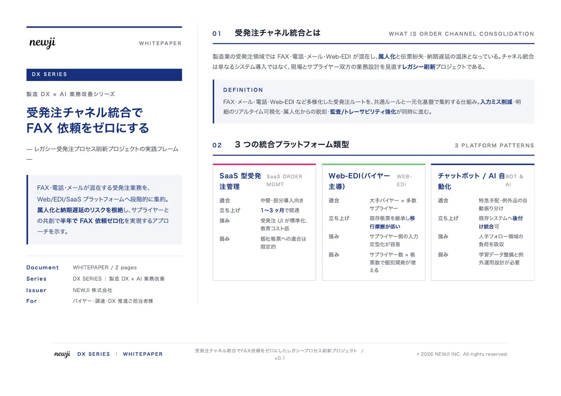
製造業の現場で使える実務資料(PDF)を無料でお届けします。"こんな資料が届きます" ↓ 下のボタンからどうぞ。
PRODUCT — 製造業向け 調達・受発注クラウド
この記事の課題、
newji で解決しませんか?
newji は、製造業の調達・受発注に特化したクラウド/AIエージェント。見積依頼・発注書作成・進捗管理・承認をひとつの画面に集約し、AIが比較と異常検知を担当。最後の「GO」だけ人が押す仕組みです。
- 見積〜発注〜納期を一元管理。催促・転記のムダをゼロに
- AIが相見積もり比較と異常検知。あなたは判断だけに集中
- 取引先は「招待」で完全無料。自社コストだけで取引先ごとデジタル化
※ 取引先から招待された企業様は完全無料でご利用いただけます
関連記事
-

Transforming Modern Electronics: Unleashing the Potential of Silicon-on-Insulator (SOI) Technology for Enhanced Industry Recognition and Market Expansion
-

Evolution of 3D Printing Technology Revolutionizing Manufacturing
-

Manufacturing Process Flow Optimization is the Secret to Increasing Efficiency and Productivity in Manufacturing
-

MOSFET(Metal-Oxide-Semiconductor Field-Effect Transistor)の最新技術と製造業での応用
-
Building a Digital Infrastructure to Support the Next Generation of Manufacturing
-
Kaizen! The Power of Continuous Process Improvement in Manufacturing

 調達購買アウトソーシング
 OEM/ODM 生産委託
 NEWJI DX
 受発注AIエージェント