

- お役立ち記事
- High-Temperature Packaging and Thermal Design for Power Semiconductors

High-Temperature Packaging and Thermal Design for Power Semiconductors

目次
Understanding High-Temperature Packaging
High-temperature packaging in power semiconductors is crucial for ensuring optimal performance and reliability under extreme conditions.
As power electronics continue to evolve, there is an increasing demand for devices that can operate at higher temperatures.
This is particularly significant in industries such as automotive, aerospace, and renewable energy, where components are often subjected to harsh environments.
High-temperature packaging involves selecting materials and design strategies that can withstand elevated temperatures without degrading performance.
Materials for High-Temperature Environments
The choice of materials in high-temperature packaging plays a pivotal role in a semiconductor’s performance.
Traditional materials like silicon have limitations when exposed to extreme heat.
Thus, newer materials like silicon carbide (SiC) and gallium nitride (GaN) are preferred for their superior thermal properties.
These materials not only withstand higher temperatures but also improve efficiency and reduce power loss.
Additionally, they are more durable, reducing the risk of failure in high-demand applications.
The Role of Thermal Interfaces
A thermal interface is crucial in managing the heat generated by power semiconductors.
In high-temperature packaging, the thermal interface material (TIM) must efficiently conduct heat away from the semiconductor to prevent overheating.
Materials such as phase-change materials and advanced thermally conductive pastes are often used.
These materials fill the microscopic gaps between surfaces, enhancing thermal conductivity and maintaining performance at high temperatures.
Thermal Design Strategies
Designing for thermal management is a critical aspect of developing power semiconductor devices.
It involves a comprehensive approach to ensure that heat is effectively dissipated to keep the device within safe temperature limits.
Heat Sink Integration
One of the most common methods of thermal management is the integration of heat sinks.
These components increase the surface area available for heat dissipation, allowing for more efficient cooling.
The design and material of a heat sink are crucial.
For instance, aluminum and copper are often used due to their excellent thermal conductivity.
Ensuring a proper fit and connection between the heat sink and the device is essential to optimize performance.
Advanced Cooling Techniques
Beyond traditional heat sinks, advanced cooling techniques are being developed to meet the demands of high-temperature applications.
Liquid cooling systems, for example, provide an alternative to air-based systems, offering more efficient heat transfer.
These systems circulate coolant through channels to absorb and move heat away from the device.
Another approach is thermal electric cooling, which uses electric current to move heat from one side of a device to another, providing precise temperature control.
Simulation and Testing
Before implementing any thermal design strategy, simulation and testing are critical.
Computer-aided design (CAD) tools allow engineers to model thermal performance and predict how a device will behave under different conditions.
Such simulations can identify potential hotspots and inefficiencies in the design.
Physical testing complements this process by providing real-world data to validate the simulated results, ensuring that the thermal management system is effective.
Challenges and Future Directions
While significant advancements have been made in high-temperature packaging and thermal design, challenges remain.
The push for greater power density means that more heat is generated in smaller areas, complicating thermal management.
Additionally, the cost of materials like SiC and GaN can be prohibitive, especially in large-scale manufacturing.
However, ongoing research is exploring new materials and design approaches to overcome these hurdles.
The future of high-temperature packaging and thermal design looks promising, with potential developments including hybrid materials and more efficient cooling systems.
Sustainability Considerations
As we look towards future advancements, sustainability is an important consideration.
Developing materials and processes that are not only effective but also environmentally friendly is crucial.
Efforts are being made to reduce the carbon footprint of semiconductor manufacturing and to recycle materials wherever possible.
This ensures that as technology advances, it does so responsibly, with minimal impact on the environment.
Industry Collaboration and Innovation
Collaboration among industries, academia, and government organizations is key to addressing the challenges in high-temperature packaging and thermal design.
By working together, these groups can share knowledge, pool resources, and drive innovation.
Innovation through collaboration can lead to breakthroughs in material science, design, and manufacturing processes, paving the way for more efficient and reliable power semiconductors.
In conclusion, high-temperature packaging and thermal design for power semiconductors are vital for sustaining the growth of various high-tech industries.
By focusing on material science, thermal management strategies, and collaborative innovation, we can meet the increasing demands of these sectors while maintaining performance and reliability.
この記事の理解を深める
無料ホワイトペーパーをプレゼント
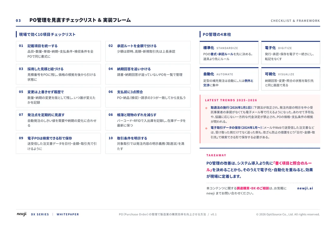
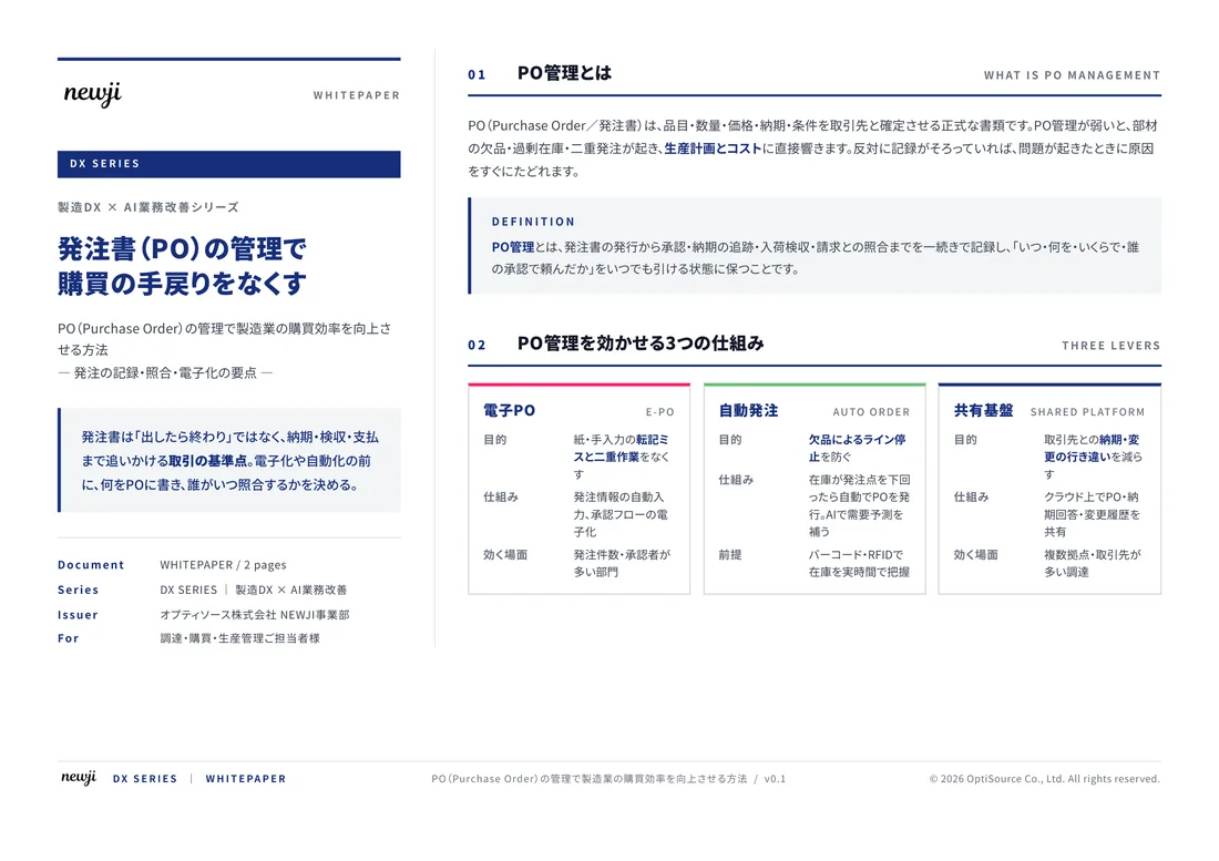
製造業の現場で使える実務資料(PDF)を無料でお届けします。"こんな資料が届きます" ↓ 下のボタンからどうぞ。
FREE DOCUMENT — サービス資料(PDF・無料)
製造業の見積・受発注クラウド
「Newji one」とは
Newji one は、製造業の調達・受発注に特化したクラウド/AIエージェント。見積依頼・発注書作成・進捗管理・承認をひとつの画面に集約し、AIが比較と異常検知を担当。最後の「GO」だけ人が押す仕組みです。
▶ 製造業の見積・受発注クラウド「Newji one」を、資料で見る(PDF・無料)
- 見積〜発注〜納期を一元管理。催促・転記のムダをゼロに
- AIが相見積もり比較と異常検知。あなたは判断だけに集中
- 取引先は「招待」で完全無料。自社コストだけで取引先ごとデジタル化
※ 取引先から招待された企業様は完全無料でご利用いただけます
関連記事
-
Transforming Modern Electronics: Unleashing the Potential of Silicon-on-Insulator (SOI) Technology for Enhanced Industry Recognition and Market Expansion
-

Power Appsで作る!簡易的な工場巡回アプリ
-
Power Automateで挑戦!製造業務フローの自動化
-
Power BIで始める!製造業KPIダッシュボードの作成
-

Microsoftパワープラットフォーム活用企業との事業連携方法
-

Saving Time and Money in Manufacturing Leads to Efficient Material Handling
 NEWJI総研
 OEM/ODM 生産委託
 AI/DX支援
 見積・発注クラウド Newji one
受発注が増えるほど、入力・確認・催促が重くなる。
受発注管理を“仕組み化“して、ミスと工数を削減しませんか。
見積・発注・納期まで一元管理できます。