

- お役立ち記事
- Ultra-precise and highly efficient micro surface processing technology and application examples of functional surface creation

その単価は妥当か。
AI が根拠付きで分析。
相見積の比較も発注も進捗管理も、ひとつの画面に。

Ultra-precise and highly efficient micro surface processing technology and application examples of functional surface creation

目次
Introduction to Ultra-Precise Micro Surface Processing
Micro surface processing is a revolutionary technological advancement that significantly impacts various industries by providing precision and efficiency in developing functional surfaces.
This advanced technique enhances the material surfaces’ physical, mechanical, and chemical properties, elevating their performance for specific applications.
The continuous evolution of micro surface processing technology offers new possibilities in manufacturing, engineering, healthcare, and electronics.
The Importance of Surface Characteristics
Surface characteristics play a crucial role in determining the performance and lifespan of a material or product.
Surface texture, roughness, hardness, and chemistry can influence a range of properties, including wear resistance, friction, adhesion, and corrosion resistance.
Micro surface processing allows for precise control of these attributes, leading to the creation of surfaces with tailor-made properties for specific uses.
Industries reliant on high-performance materials, such as aerospace, automotive, and medical devices, greatly benefit from these advancements.
Current Techniques in Micro Surface Processing
Micro surface processing encompasses a variety of techniques, each tailored to achieve specific property enhancements in materials.
Laser Surface Engineering
One of the most prevalent methods, laser surface engineering uses focused laser beams to modify surface properties.
This technique can create micro-textures and patterns that improve a material’s friction, reflectivity, and biocompatibility.
Applications range from medical implants, where enhanced biocompatibility is vital, to automobiles, where reduced friction can lead to less energy consumption.
Electrochemical Machining (ECM)
ECM is another widely used technique for micro surface processing.
It utilizes electrical currents and electrolytic fluids to remove material at the microscale, allowing for the creation of complex geometries and high surface finish.
This non-contact method is particularly useful for processing hard metals where traditional machining proves challenging.
Applications for ECM include precision component fabrication in the aerospace and defense sectors.
Photolithography
Primarily used in the electronics industry, photolithography employs light to transfer geometric patterns onto a substrate.
This method is essential for the production of integrated circuits and microelectromechanical systems (MEMS).
Photolithography enables the fabrication of extremely small and complex structures crucial for modern technologies like smartphones and computers.
Applications of Functional Surface Creation
The ability to create surfaces with specific functional properties has opened up a plethora of opportunities across different fields.
Medical Industry
In the medical sector, micro surface processing is pivotal in developing devices and implants that must integrate seamlessly with biological tissues.
Enhancing surface properties like roughness and chemistry improves biocompatibility and osseointegration, resulting in more effective and longer-lasting implants.
Functional surfaces are also used in surgical instruments to minimize friction and improve durability.
Automotive and Aerospace
In the automotive and aerospace industries, functional surface creation enhances component performance by reducing friction and wear.
This leads to lower maintenance costs, improved fuel efficiency, and extended lifespan of vehicles and aircraft components.
Micro surface processing also contributes to weight reduction by enabling the use of advanced materials like composites and lightweight metals.
Electronics and Semiconductors
The demand for miniaturized electronics with enhanced functionality drives the need for precise micro surface processing.
Complex microstructures on semiconductor wafers increase device efficiency and performance.
Functional surfaces in electronics also improve thermal management, essential for high-performance computing and communication devices.
Environmental and Economic Benefits
Beyond technological advancements, micro surface processing offers significant environmental and economic benefits.
Reduced Material Waste
The precision of micro surface processing minimizes material waste, leading to more sustainable manufacturing practices.
Less material removal and lower energy consumption during production contribute to a smaller carbon footprint.
Enhanced Product Durability
By improving surface properties, products last longer and require less frequent replacement, further reducing waste and conserving resources.
This durability extends to various applications, from consumer electronics to industrial machinery.
Cost Efficiency
The improved efficiency and performance of components lead to long-term cost savings.
Investing in micro surface processing can result in reduced operational costs and increased product reliability, providing a competitive edge to companies across sectors.
Future Prospects and Challenges
The future of ultra-precise micro surface processing holds immense promise, with ongoing research paving the way for new materials and processes.
The integration of artificial intelligence and machine learning offers prospects for automated and intelligent surface modification, enhancing efficiency and innovation.
However, challenges remain in scaling these technologies for mass production while maintaining precision and reliability.
Continued advancements in equipment, process control, and material sciences are essential for overcoming these hurdles.
Conclusion
Ultra-precise and highly efficient micro surface processing is transforming the landscape of materials engineering and manufacturing.
Its ability to tailor surface properties for specific applications opens up new possibilities for innovation and sustainability.
As technology progresses, the potential for micro surface processing to revolutionize industries and improve everyday life continues to grow, making it a cornerstone of modern scientific and technological advancement.
この記事の理解を深める
無料ホワイトペーパーをプレゼント
製造業の現場で使える実務資料(PDF)を無料でお届けします。"こんな資料が届きます" ↓ 下のボタンからどうぞ。
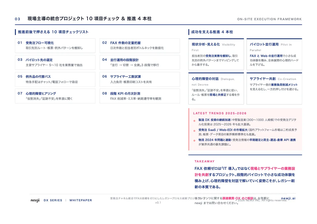
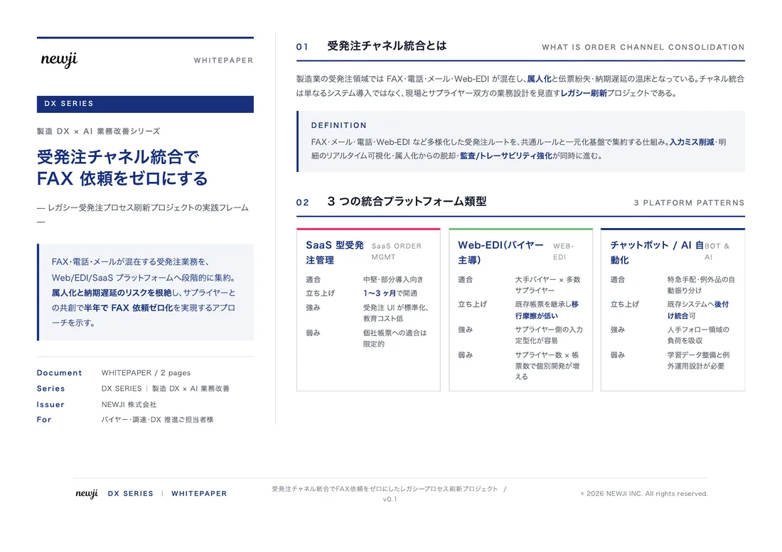
FREE DOCUMENT — サービス資料(PDF・無料)
製造業の見積・受発注クラウド
「Newji one」とは
Newji one は、製造業の調達・受発注に特化したクラウド/AIエージェント。見積依頼・発注書作成・進捗管理・承認をひとつの画面に集約し、AIが比較と異常検知を担当。最後の「GO」だけ人が押す仕組みです。
▶ 製造業の見積・受発注クラウド「Newji one」を、資料で見る(PDF・無料)
- 見積〜発注〜納期を一元管理。催促・転記のムダをゼロに
- AIが相見積もり比較と異常検知。あなたは判断だけに集中
- 取引先は「招待」で完全無料。自社コストだけで取引先ごとデジタル化
※ 取引先から招待された企業様は完全無料でご利用いただけます
関連記事
-

Transforming Modern Electronics: Unleashing the Potential of Silicon-on-Insulator (SOI) Technology for Enhanced Industry Recognition and Market Expansion
-

MEMS(Micro-Electro-Mechanical Systems)の技術と製造業での応用例
-
超高真空 (Ultra-high Vacuum) の技術と製造業での利用方法
-
“Ultra-High Performance Concrete (UHPC)を用いた調達購買革新: 製造業の次世代戦略”
-
超高真空 (Ultra-high Vacuum) 技術で製造業の革新を実現する調達購買戦略
-
スマート鍵探しタグOEMが家族共有を容易にするUltra-wideband精密測位
 NEWJI総研
 OEM/ODM 生産委託
 AI/DX支援
 見積・発注クラウド Newji one
受発注が増えるほど、入力・確認・催促が重くなる。
受発注管理を“仕組み化“して、ミスと工数を削減しませんか。
見積・発注・納期まで一元管理できます。