

- お役立ち記事
- Impedance Control and High-Speed Signal Design for Printed Circuit Boards

その単価は妥当か。
AI が根拠付きで分析。
相見積の比較も発注も進捗管理も、ひとつの画面に。

Impedance Control and High-Speed Signal Design for Printed Circuit Boards

Printed circuit boards (PCBs) are crucial components in modern electronic devices.
Their design is essential for achieving optimal performance, especially when it comes to high-speed signal processing.
Impedance control is a key aspect of PCB design that ensures signals can be transmitted without interference or loss.
In this article, we will explore how impedance control works and provide practical tips for high-speed signal design on PCBs.
目次
Understanding Impedance Control in PCBs
Impedance is the total resistance that a circuit offers to the flow of alternating current (AC) at a specific frequency.
In the context of PCBs, impedance control ensures that the signal can travel through conductors and dielectrics with minimal reflection or loss.
It requires careful attention to materials, trace width, and spacing.
Let’s delve into the components of impedance control.
The Role of Dielectric Materials
Dielectric materials insulate conductive traces on a PCB.
These materials have dielectric constants (Dk), which affect the impedance of the traces.
Higher Dk values mean higher capacitance and lower impedance, and vice versa.
Selecting the right dielectric material is crucial for maintaining the desired impedance level for high-speed signals.
Trace Width and Spacing
Trace width and spacing are also vital in controlling impedance.
Wider traces have lower impedance, while narrower traces have higher impedance.
Spacing between traces affects coupling, which can lead to crosstalk and interference.
Using a controlled impedance calculator helps designers determine the correct trace width and spacing for their specific requirements.
Layer Stackup
Layer stackup refers to the arrangement of conductive and insulating layers in a PCB.
A well-designed layer stackup minimizes impedance variations and ensures signal integrity.
Designers often use ground planes below signal layers to provide a consistent return path, reducing noise and maintaining stable impedance.
High-Speed Signal Design Techniques
High-speed signal design in PCBs involves minimizing signal loss, interference, and reflection.
Here are some essential techniques for achieving robust high-speed signal transmission.
Maintaining Signal Integrity
Signal integrity is the preservation of signal quality over its transmission path.
For high-speed circuits, maintaining signal integrity requires strict control over impedance.
Impedance mismatches can result in signal reflections, leading to data errors and reduced performance.
Using tools like time-domain reflectometry (TDR) can help identify and fix impedance mismatches.
Differential Signaling
Differential signaling involves transmitting signals over pairs of traces instead of single-ended signals.
This technique reduces the impact of electromagnetic interference and crosstalk.
Each pair consists of a positive (D+) and negative (D-) signal that complements each other, thus canceling out noise.
Designers must match the length and impedance of these pairs to prevent skew and ensure synchronization.
Microstrip and Stripline Configurations
Traces can be designed using microstrip or stripline configurations.
Microstrip traces are on the outer layers of the PCB and have one side exposed to air, affecting their impedance.
Stripline traces are embedded between layers of dielectric material, offering better control over impedance and signal integrity.
Choosing the appropriate configuration depends on the specific needs of the design.
Minimizing Crosstalk
Crosstalk is unwanted coupling between adjacent traces.
It can cause data corruption and signal integrity issues.
To minimize crosstalk, designers should use adequate spacing between traces and employ ground planes.
Routing high-speed signals on different layers and using differential pairs can further reduce the risk of crosstalk.
Best Practices for Impedance Control and High-Speed Design
Implementing best practices ensures reliable performance of high-speed PCBs.
Here are some guidelines to follow.
Use Impedance Controlled PCBs
Opt for PCBs with manufactured impedance control.
These boards are fabricated with consistent trace width, spacing, and dielectric materials, minimizing impedance variations.
Consult your PCB manufacturer for their impedance control capabilities and specifications.
Careful Layout and Routing
Plan the layout carefully to avoid unnecessary bends and vias, which can affect impedance.
Route high-speed signals as straight as possible and use smooth, gradual bends with a larger radius.
Minimize the use of vias as they introduce impedance discontinuities.
Simulation and Testing
Use simulation tools to model your PCB design and identify potential issues before fabrication.
Simulations help verify impedance control, signal integrity, and crosstalk levels.
After manufacturing, employ testing methods like TDR and oscilloscope measurements to validate your design.
Documentation and Communication
Provide clear documentation to your PCB manufacturer regarding impedance requirements.
Include detailed layer stackup, trace width, and spacing information.
Effective communication ensures the final product meets your design specifications.
Conclusion
Impedance control and high-speed signal design are integral to the performance of modern PCBs.
By understanding the principles of impedance, selecting appropriate materials, and following best design practices, engineers can achieve optimal signal integrity and minimal interference.
Implementing these techniques ensures that electronic devices function reliably, even at high speeds, meeting the ever-growing demands of today’s technology.
この記事の理解を深める
無料ホワイトペーパーをプレゼント
製造業の現場で使える実務資料(PDF)を無料でお届けします。"こんな資料が届きます" ↓ 下のボタンからどうぞ。
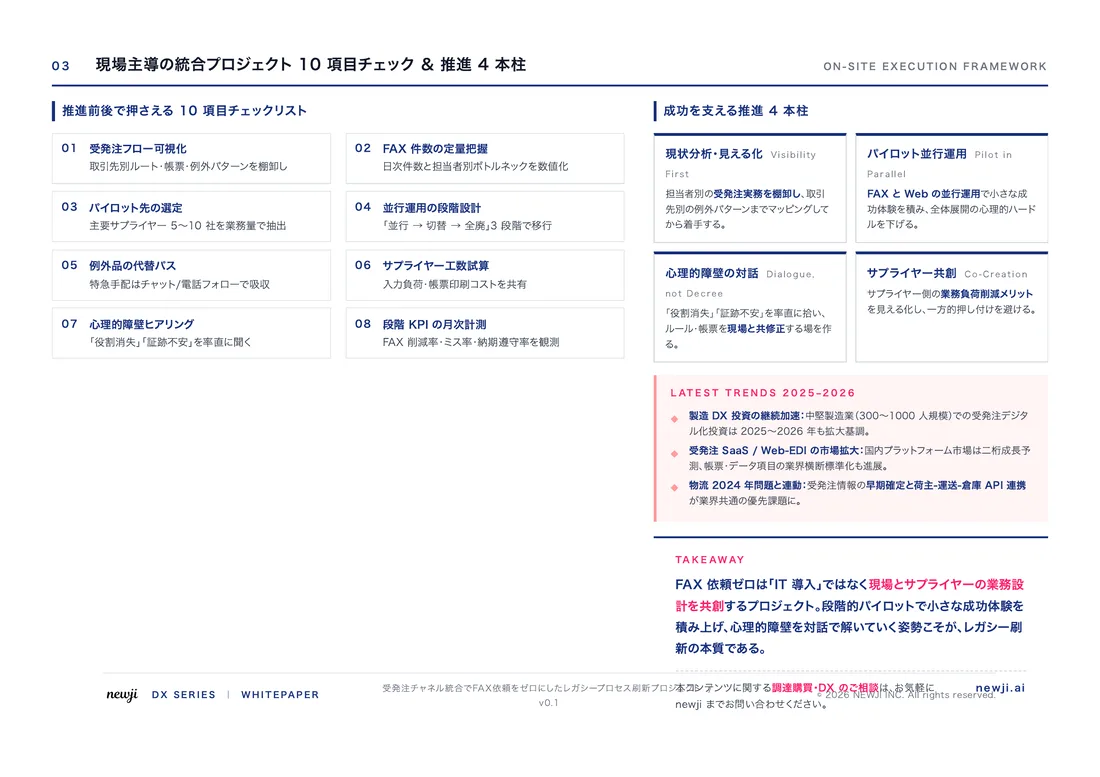
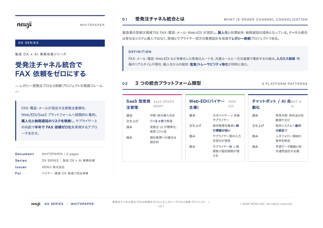
FREE DOCUMENT — サービス資料(PDF・無料)
製造業の見積・受発注クラウド
「Newji one」とは
Newji one は、製造業の調達・受発注に特化したクラウド/AIエージェント。見積依頼・発注書作成・進捗管理・承認をひとつの画面に集約し、AIが比較と異常検知を担当。最後の「GO」だけ人が押す仕組みです。
▶ 製造業の見積・受発注クラウド「Newji one」を、資料で見る(PDF・無料)
- 見積〜発注〜納期を一元管理。催促・転記のムダをゼロに
- AIが相見積もり比較と異常検知。あなたは判断だけに集中
- 取引先は「招待」で完全無料。自社コストだけで取引先ごとデジタル化
※ 取引先から招待された企業様は完全無料でご利用いただけます




 NEWJI総研
 OEM/ODM 生産委託
 AI/DX支援
 見積・発注クラウド Newji one
受発注が増えるほど、入力・確認・催促が重くなる。
受発注管理を“仕組み化“して、ミスと工数を削減しませんか。
見積・発注・納期まで一元管理できます。