

- お役立ち記事
- Basics and Latest Technologies in Semiconductor Processes

その単価は妥当か。
AI が根拠付きで分析。
相見積の比較も発注も進捗管理も、ひとつの画面に。

Basics and Latest Technologies in Semiconductor Processes

目次
Understanding Semiconductor Processes
Semiconductors are the backbone of modern electronics, found in devices ranging from smartphones to cars.
Understanding semiconductor processes is essential as they form the building blocks of these devices.
The process involves several stages that transform raw silicon into intricate and functional semiconductor chips.
The Basics of Semiconductor Fabrication
The semiconductor fabrication process can be divided into several key steps.
First, raw silicon is transformed into silicon wafers.
These wafers serve as the substrate upon which circuits are built.
Next, the photolithography process imprints intricate circuit designs onto the wafer using light and chemical treatments.
The photoresist material applied to the wafer undergoes exposure to ultraviolet light, which creates patterns according to the specific blueprint required for each chip.
Key Steps in Semiconductor Manufacturing
1. Doping
Doping is a critical technique used to modify the electrical properties of semiconductors.
By introducing impurities into pure silicon, manufacturers can control the flow of electric current through the material.
This step is essential for creating components like transistors, which are necessary for amplification and switching electronic signals.
2. Etching
Etching is another crucial stage where unwanted material is removed from the wafer’s surface, leaving behind the desired pattern.
There are two main etching techniques: wet etching, which uses liquid chemicals, and dry etching, which employs gaseous substances.
Both methods have their advantages depending on the required precision and materials involved.
3. Deposition
During the deposition process, thin layers of materials are added to the wafer’s surface.
These layers might be conductors, insulators, or semiconductors depending on the intended function of the chip.
Common deposition techniques include Chemical Vapor Deposition (CVD) and Physical Vapor Deposition (PVD).
Latest Technologies in Semiconductor Processes
As technology advances, semiconductor processes continue to evolve.
Manufacturers constantly strive for efficiency, reduced size, and increased performance.
1. Extreme Ultraviolet Lithography (EUV)
EUV is a groundbreaking technology that allows for smaller and more accurate patterning of semiconductor devices.
Using extreme ultraviolet wavelengths, EUV enables the creation of circuits at a scale previously unattainable with standard photolithography.
This technology is essential for producing advanced chips required for high-performance computing and AI applications.
2. 3D FinFET Transistors
3D Fin Field-Effect Transistors (FinFET) represent a significant leap in transistor technology.
Unlike traditional planar transistors, FinFETs have a three-dimensional structure, reducing power consumption while enhancing performance.
This innovation is particularly important as devices get smaller, requiring efficient transistors to maintain high-speed operations.
3. Advanced Packaging
Advanced packaging techniques are crucial for enhancing the performance and functionality of semiconductor devices.
Methods such as Chiplets and System-in-Package (SiP) allow multiple chips to be integrated into a single package, improving efficiency and scalability.
These techniques enable the production of more powerful and compact electronic devices.
The Future of Semiconductor Processes
As we advance towards a more connected world, the demand for efficient semiconductor processes will continue to grow.
Emerging technologies like quantum computing and neuromorphic chips are pushing the boundaries of what’s possible in semiconductor fabrication.
Sustainability in Semiconductor Production
One of the significant challenges facing semiconductor manufacturing is sustainability.
The industry is focusing on reducing the environmental impact by implementing cleaner technologies and optimizing resource use.
Recycling and reclaiming materials are becoming increasingly essential to minimize waste and energy consumption.
Investments in Research and Development
Investing in research and development is crucial for the semiconductor industry’s future.
Governments and companies worldwide are channeling resources towards innovation in semiconductor technologies.
Breakthroughs in material science, process efficiency, and new architectures are essential to keep pace with the growing demand for faster, smaller, and more efficient devices.
Conclusion
The world of semiconductor processes is continuously evolving, driven by technological innovation and the demand for sustainable solutions.
From the basics of photolithography and doping to cutting-edge advancements in EUV and FinFET technologies, each aspect plays a vital role in creating the chips that power our modern lives.
As we look to the future, collaboration between industry leaders and researchers will be key to overcoming challenges and driving progress in semiconductor fabrication.
Whether you’re a tech enthusiast or a professional in the field, understanding these processes helps appreciate the intricate work behind the devices we often take for granted.
この記事の理解を深める
無料ホワイトペーパーをプレゼント
製造業の現場で使える実務資料(PDF)を無料でお届けします。"こんな資料が届きます" ↓ 下のボタンからどうぞ。
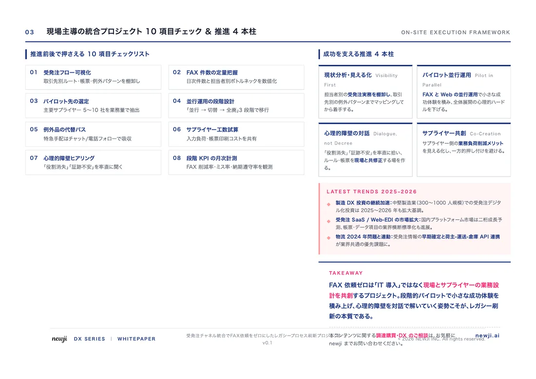
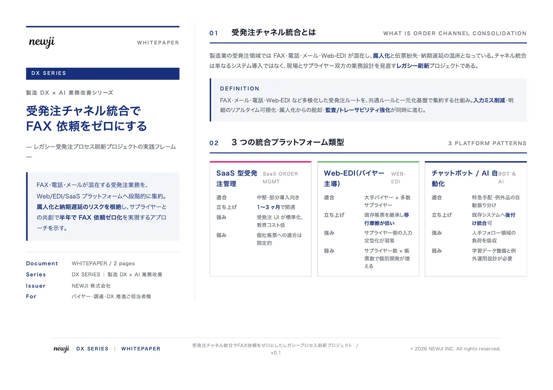
FREE DOCUMENT — サービス資料(PDF・無料)
製造業の見積・受発注クラウド
「Newji one」とは
Newji one は、製造業の調達・受発注に特化したクラウド/AIエージェント。見積依頼・発注書作成・進捗管理・承認をひとつの画面に集約し、AIが比較と異常検知を担当。最後の「GO」だけ人が押す仕組みです。
▶ 製造業の見積・受発注クラウド「Newji one」を、資料で見る(PDF・無料)
- 見積〜発注〜納期を一元管理。催促・転記のムダをゼロに
- AIが相見積もり比較と異常検知。あなたは判断だけに集中
- 取引先は「招待」で完全無料。自社コストだけで取引先ごとデジタル化
※ 取引先から招待された企業様は完全無料でご利用いただけます
関連記事
-

Transforming Modern Electronics: Unleashing the Potential of Silicon-on-Insulator (SOI) Technology for Enhanced Industry Recognition and Market Expansion
-

Silicon Carbideを活用した次世代製造プロセスの最適化方法
-

EUV技術革命!製造業が集う最前線の現場レポート
-
【製造業必見】調達購買部門が押さえておくべき最新露光装置の選定ポイントとは?
-
Silicon-on-Insulator (SOI)の革新が営業力を強化する手法と戦略
-

ALD(原子層堆積)/ALE(原子層エッチング)技術の基礎と高機能薄膜への応用
 NEWJI総研
 OEM/ODM 生産委託
 AI/DX支援
 見積・発注クラウド Newji one
受発注が増えるほど、入力・確認・催促が重くなる。
受発注管理を“仕組み化“して、ミスと工数を削減しませんか。
見積・発注・納期まで一元管理できます。