

- お役立ち記事
- Circuit design that allows the operation of a single FPGA and the coordination of the CPU

その単価は妥当か。
AI が根拠付きで分析。
相見積の比較も発注も進捗管理も、ひとつの画面に。

Circuit design that allows the operation of a single FPGA and the coordination of the CPU

目次
Understanding FPGA and CPU Coordination
Field Programmable Gate Arrays (FPGAs) have emerged as significant players in the realm of electronic design due to their flexibility and high performance.
They are used frequently in various applications such as telecommunications, automotive systems, and consumer electronics.
Understanding how to effectively coordinate an FPGA with a CPU can lead to more powerful and efficient systems.
In this article, we will delve into the concepts, benefits, and methodologies involved in designing a circuit that facilitates the operation of a single FPGA while coordinating it with a CPU.
What is an FPGA?
An FPGA is a type of semiconductor device that is based around a matrix of configurable logic blocks (CLBs) connected via programmable interconnects.
This configuration allows it to be programmed and reconfigured to perform a variety of computational tasks.
Unlike traditional processors, FPGAs do not have a fixed set of operations they can perform.
Instead, they are highly adaptable and can be customized for specific tasks.
This flexibility makes them ideal for applications that require rapid prototyping and algorithmic changes.
The Role of a CPU in System Design
A Central Processing Unit (CPU) is the brain of a computer, handling all instructions received from hardware and software running on the computer.
When acting in combination with an FPGA, a CPU can handle general-purpose processing while the FPGA takes care of specialized tasks.
This symbiotic relationship can maximize the performance of the system.
The CPU provides the infrastructure, managing input/output operations, memory allocation, and other general computing functions.
Meanwhile, the FPGA can be fine-tuned to execute specific tasks faster than the CPU.
Benefits of FPGA and CPU Coordination
There are several advantages to coordinating an FPGA with a CPU.
First, it can significantly enhance computational efficiency.
FPGAs can perform parallel processing, making them highly efficient at executing complex algorithms compared to traditional CPUs that operate serially.
This capability is especially beneficial in high-performance computing environments.
Second, the flexibility of FPGAs allows for quick adaptability to changing workloads.
In fast-evolving fields like artificial intelligence and machine learning, being able to quickly update the FPGA’s configuration is a major advantage.
Additionally, utilizing both an FPGA and a CPU can help reduce latency in operations that require immediate processing, such as in real-time data analysis or edge computing applications.
Designing a Coordinated Circuit
To design a circuit that effectively coordinates an FPGA with a CPU, several key steps and considerations must be taken into account.
Understanding Requirements
Before starting the design process, it is essential to thoroughly understand the application’s requirements.
Determine which tasks would benefit from the accelerated execution capabilities of the FPGA.
Simultaneously, assess which processes are better handled by the CPU’s general-purpose nature.
Defining Communication Protocols
Effective communication between the FPGA and CPU is crucial.
Set up clear communication protocols, such as bus interfaces or memory mapping, to ensure smooth data transfer.
Protocols like AXI or Avalon can be used to establish a standardized data interface between the FPGA and the CPU.
Optimizing Data Flow
The next step involves optimizing the data flow between the FPGA and CPU.
This includes designing efficient paths for data exchange and ensuring that both components are synchronized effectively.
Consider implementing Direct Memory Access (DMA) to facilitate high-speed data transfer without burdening the CPU with routine data movement tasks.
Implementing FPGA Design
With communication and data flow considerations in place, focus on implementing the FPGA design.
Develop the necessary logic circuits within the FPGA to process the specific tasks it is intended to perform.
Test and evaluate the FPGA’s performance to ensure it meets the required specifications and functions optimally within the coordinated system.
Testing and Validation
Once the circuit design is complete, rigorous testing and validation are essential to ensure reliable operation.
This involves simulating the FPGA’s functions alongside the CPU to identify any potential bottlenecks, conflicts, or errors.
Use high-level design tools and simulation software to evaluate the system’s performance under various scenarios.
Iterative Refinement
Circuit design is often an iterative process, with testing revealing opportunities for refinement.
Adjust logic blocks, telecommunications protocols, or other parameters to improve system performance.
Through iterative testing and refinement, you can enhance the integration and coordination between the FPGA and the CPU.
Conclusion
Incorporating both an FPGA and a CPU into a single system can offer considerable performance benefits.
When these two components work effectively together, they can handle a range of tasks with speed and efficiency that neither could achieve alone.
By understanding the roles of each component, carefully designing their communication pathways, and rigorously validating the design, you can create systems that meet modern demands with impressive computational power.
Whether you’re involved in developing cutting-edge technology in telecommunications, data processing, or consumer electronics, mastering the coordination of FPGA and CPU within a circuit will undoubtedly be of great advantage.
この記事の理解を深める
無料ホワイトペーパーをプレゼント
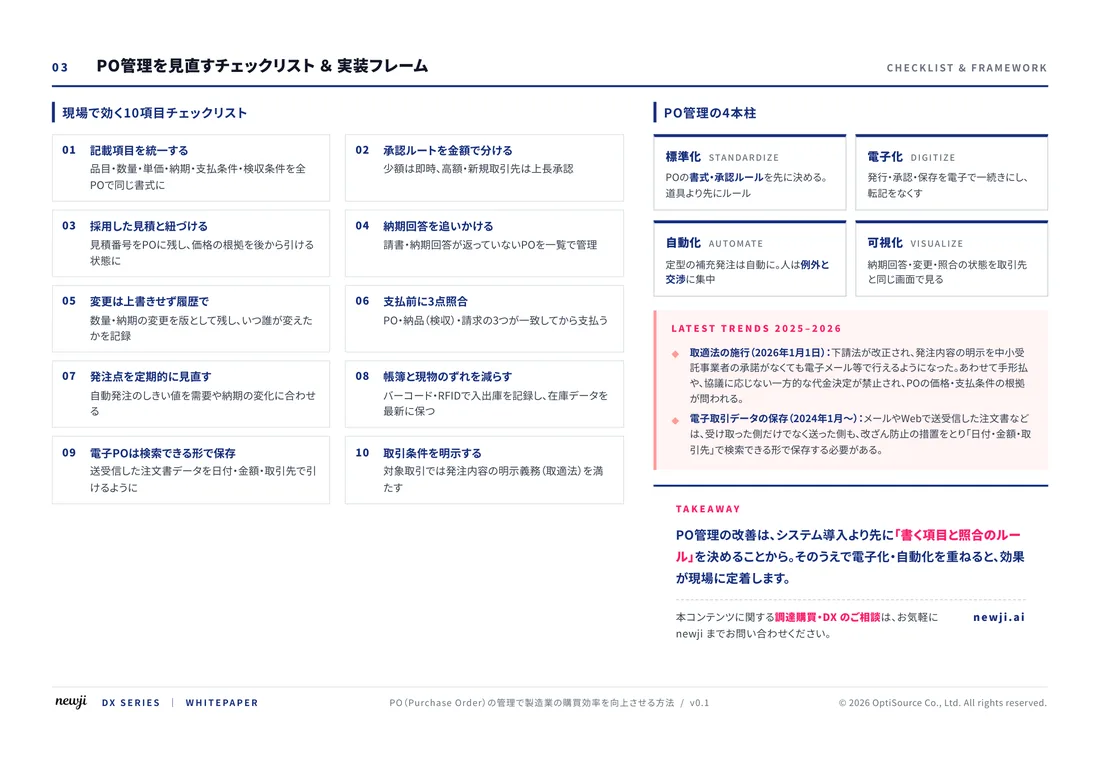
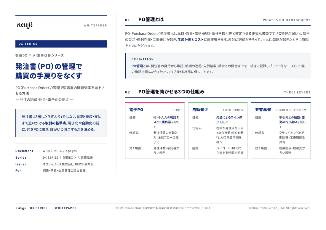
製造業の現場で使える実務資料(PDF)を無料でお届けします。"こんな資料が届きます" ↓ 下のボタンからどうぞ。
FREE DOCUMENT — サービス資料(PDF・無料)
製造業の見積・受発注クラウド
「Newji one」とは
Newji one は、製造業の調達・受発注に特化したクラウド/AIエージェント。見積依頼・発注書作成・進捗管理・承認をひとつの画面に集約し、AIが比較と異常検知を担当。最後の「GO」だけ人が押す仕組みです。
▶ 製造業の見積・受発注クラウド「Newji one」を、資料で見る(PDF・無料)
- 見積〜発注〜納期を一元管理。催促・転記のムダをゼロに
- AIが相見積もり比較と異常検知。あなたは判断だけに集中
- 取引先は「招待」で完全無料。自社コストだけで取引先ごとデジタル化
※ 取引先から招待された企業様は完全無料でご利用いただけます

 NEWJI総研
 OEM/ODM 生産委託
 AI/DX支援
 見積・発注クラウド Newji one
受発注が増えるほど、入力・確認・催促が重くなる。
受発注管理を“仕組み化“して、ミスと工数を削減しませんか。
見積・発注・納期まで一元管理できます。