

- お役立ち記事
- Fundamentals of FPGA circuit design and application to debugging and high-speed design

スタートアップから大手まで。
調達・受発注をAIで標準化。
相見積比較も進捗管理もAIが下支え。取引先は招待で完全無料。

Fundamentals of FPGA circuit design and application to debugging and high-speed design

目次
Understanding FPGAs
Field-Programmable Gate Arrays (FPGAs) are integrated circuits that can be configured by a customer or a designer after manufacturing.
They offer a flexible platform for digital circuit design, making them an essential tool for many applications, including debugging and high-speed design.
Unlike Application-Specific Integrated Circuits (ASICs), FPGAs can be reprogrammed to suit various needs and uses.
This reconfiguration capability makes FPGAs a popular choice in industries requiring intensive computations, such as telecommunications, data centers, and embedded systems.
Basic Components of FPGA Circuit Design
Starting with FPGA design might seem daunting due to its complexity.
However, understanding its basic components can make the learning process more manageable.
Logic Blocks
Logic blocks are the building blocks of FPGAs.
They consist of small units of logic gates that are capable of implementing simple logic functions.
The most common type of logic block used in FPGAs is the Look-Up Table (LUT), which can execute any logic function defined by the user.
Besides logic operations, these blocks can include sequence logic like flip-flops to store data.
Interconnects
Interconnects are the pathways that connect the logic blocks within the FPGA.
They are designed to be programmable, enabling different logic blocks to connect depending on the defined configuration.
Efficient interconnect design is crucial, as it affects the speed and performance of the FPGA.
Proper planning and organization of interconnect pathways can lead to enhanced FPGA operation.
Input/Output Blocks (IOBs)
Input/Output Blocks handle the data going in and out of the FPGA.
These blocks are designed to interface with external systems, making sure that the FPGA can communicate effectively with other devices.
IOBs can be configured to support various standards, enabling the FPGA to adapt to different voltage levels, speeds, and protocols required by external peripherals.
FPGA Design Process
The process of designing an FPGA involves several steps, which are critical for creating an effective circuit.
Specification and Planning
Successful FPGA design starts with a clear set of specifications detailing the intended function and performance parameters.
This phase involves understanding the requirements of the application, including operational speed, power consumption, and interface requirements.
Design Entry
Once the specifications are set, the design entry involves building the logic circuit on a computer using hardware description languages (HDLs) such as VHDL or Verilog.
These languages allow designers to define the complex processes and behaviors the FPGA needs to perform.
Synthesis
During synthesis, the HDL descriptions are converted into a gate-level representation, an essential step for mapping to the physical resources on the FPGA.
The goal is to optimize logic design to meet specified performance and resource constraints.
Implementation
Implementation involves mapping, placing, and routing the logical representation onto the physical FPGA hardware, ensuring that logic blocks and interconnects are properly configured.
This step is crucial for balancing performance, speed, and resource utilization.
Testing and Debugging
Testing and debugging are vital to ensuring the FPGA works as intended.
Simulation tools are used to test the logical design in virtual scenarios, checking for functionality and identifying potential issues before the hardware is deployed.
FPGA in Debugging and High-Speed Design
FPGAs offer specific advantages for debugging and high-speed applications.
Advanced Debugging Capabilities
FPGAs allow engineers to embed custom logic analyzers to pinpoint issues in real-time.
This feature enhances the ability to detect faults within a system, leading to better diagnostics and shorter development cycles.
Moreover, the FPGA’s reprogrammable nature enables rapid iteration, allowing for quick adjustments and testing without needing extensive hardware changes.
High-Speed Design Applications
FPGAs are well-suited for high-speed design due to their parallel processing capabilities and high bandwidth.
They can handle multiple tasks simultaneously, which is suitable for applications such as networking, video processing, and real-time data analysis.
FPGAs are also designed to be overclocked, meaning they can operate at higher speed than standard processing units, improving performance for time-sensitive applications.
Conclusion
FPGAs represent a powerful tool in modern circuit design, offering versatility through reprogrammability.
Understanding their core components and design processes allows designers to apply them effectively in debugging and high-speed applications.
As technology advances, the role of FPGAs will continue to expand, providing flexible solutions across diverse technical fields.
この記事の理解を深める
無料ホワイトペーパーをプレゼント
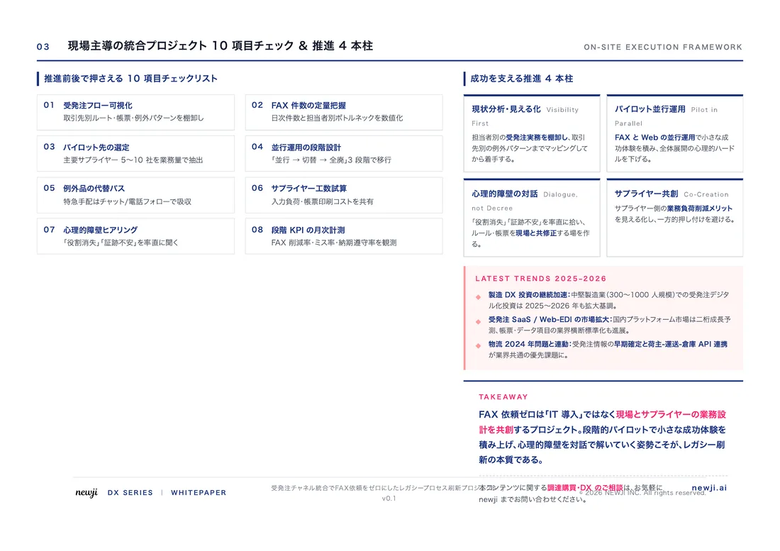
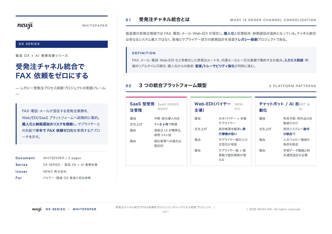
製造業の現場で使える実務資料(PDF)を無料でお届けします。"こんな資料が届きます" ↓ 下のボタンからどうぞ。
PRODUCT — 製造業向け 調達・受発注クラウド
この記事の課題、
newji で解決しませんか?
newji は、製造業の調達・受発注に特化したクラウド/AIエージェント。見積依頼・発注書作成・進捗管理・承認をひとつの画面に集約し、AIが比較と異常検知を担当。最後の「GO」だけ人が押す仕組みです。
- 見積〜発注〜納期を一元管理。催促・転記のムダをゼロに
- AIが相見積もり比較と異常検知。あなたは判断だけに集中
- 取引先は「招待」で完全無料。自社コストだけで取引先ごとデジタル化
※ 取引先から招待された企業様は完全無料でご利用いただけます


 調達購買アウトソーシング
 OEM/ODM 生産委託
 NEWJI DX
 受発注AIエージェント