

- お役立ち記事
- Fundamentals of silicon photonics and important points in integrated circuit technology and integrated process construction

スタートアップから大手まで。
調達・受発注をAIで標準化。
相見積比較も進捗管理もAIが下支え。取引先は招待で完全無料。

Fundamentals of silicon photonics and important points in integrated circuit technology and integrated process construction

Silicon photonics is a burgeoning field that merges the technological prowess of photonics with the foundational elements of silicon-based electronics.
As we delve into the fundamentals of silicon photonics, it’s essential to comprehend the integral connection it shares with integrated circuit technology and the associated processes that accompany its construction.
目次
Understanding Silicon Photonics
Silicon photonics leverages light (photons) to perform functions that are typically handled by electrons in silicon-based devices.
This technology utilizes silicon as a medium to manipulate, transmit, and detect light.
One of the standout advantages of silicon photonics is its potential to significantly increase data transmission speeds while reducing power consumption, thus driving efficiency in communication systems.
The core aim of silicon photonics is to integrate optical and electronic functions on a single chip, known as photonic integrated circuits (PICs).
These circuits offer remarkable advantages in terms of scalability and cost-effectiveness.
Since silicon is the most abundant element in the Earth’s crust and extensively utilized in the semiconductor industry, silicon photonics capitalizes on existing manufacturing infrastructure to lower production costs.
The Intersection with Integrated Circuit Technology
The interplay between silicon photonics and integrated circuit technology is crucial for advancing modern electronic applications.
Integrated circuit technology refers to the microfabrication processes used to create a compact array of electronic devices and circuits on a single semiconductor chip.
When combined with the benefits of photonics, silicon-based integrated circuits can achieve groundbreaking performance in data transfer and processing.
The integration of photonic components with electronic circuits allows for more efficient data processing and communication.
For instance, in data centers, silicon photonics can improve the speed of server connections, enabling faster data transfer rates across networks.
This is achieved by replacing conventional electrical pathways with photonic channels, which can carry much more data over longer distances without significant energy loss.
Benefits of Integrating Photonics and Electronics
1. **Speed and Bandwidth:** Photonics provides a significant advantage in terms of speed and bandwidth.
Light can carry multiple signals simultaneously over various wavelengths, allowing more data to be transferred at higher speeds.
2. **Energy Efficiency:** With reduced energy loss compared to electronic systems, photonic circuits noticeably improve energy efficiency.
This is particularly beneficial in large-scale data centers where power consumption is a major concern.
3. **Scalability:** Utilizing existing silicon fabrication processes ensures that photonic integrated circuits can be mass-produced just like their electronic counterparts.
This makes widespread adoption more feasible and cost-effective.
Key Points in Integrated Process Construction
Building a successful silicon photonic integrated circuit involves several critical processes.
Understanding these steps helps to unlock the true potential of this technology.
Substrate Preparation
The foundation of any silicon photonics project begins with substrate preparation.
A high-quality silicon wafer is essential to serve as the backbone for the integrated circuit.
This involves processes like wafer thinning, polishing, and cleaning to ensure a pristine starting point for subsequent steps.
Waveguide Fabrication
Waveguides are integral components of photonic circuits, responsible for directing light signals across the chip.
These are typically fabricated using advanced lithography techniques followed by etching processes to create precise pathways.
Ensuring low-loss transmission in waveguides is crucial, as this directly impacts the efficiency and performance of the integrated circuit.
Integration of Active and Passive Devices
A robust silicon photonics circuit incorporates both active and passive elements.
Active devices like modulators are responsible for encoding data onto light signals.
Meanwhile, passive components such as filters and couplers aid in signal management without the need for external power.
The integration of these components requires meticulous alignment and bonding processes.
Advanced packaging techniques are employed to connect these devices and their electronic counterparts seamlessly.
Ensuring compatibility between photonic and electronic components is critical to achieving optimal functionality.
Challenges and Future Directions
Despite its promise, silicon photonics faces several challenges that need addressing.
Thermal Management
The thermal effects within silicon chips can alter the performance of photonic devices, leading to signal degradation.
Overcoming these challenges involves developing better thermal handling processes and materials that can efficiently dissipate heat.
Material Limitations
Silicon has some inherent material limitations, particularly in terms of its inability to efficiently generate laser light.
Ongoing research focuses on integrating other materials like germanium to complement silicon, broadening its photonic capabilities.
Scaling and Integration
As the scale of photonic integrated circuits increases, so does the complexity of their integration with electronics.
Efforts are being made to refine these integration techniques to ensure stable and reliable circuit performance.
Conclusion
Silicon photonics represents a transformative approach to enhancing our electronic systems with the speed and efficiency of light.
By marrying the principles of photonics with established silicon-based circuit technology, we uncover new pathways for innovation in data transmission and processing.
As the field matures, overcoming existing challenges will be pivotal in unlocking the full potential of silicon photonics.
Continued research and development are necessary to ensure that this technology becomes a cornerstone of modern electronic systems.
この記事の理解を深める
無料ホワイトペーパーをプレゼント
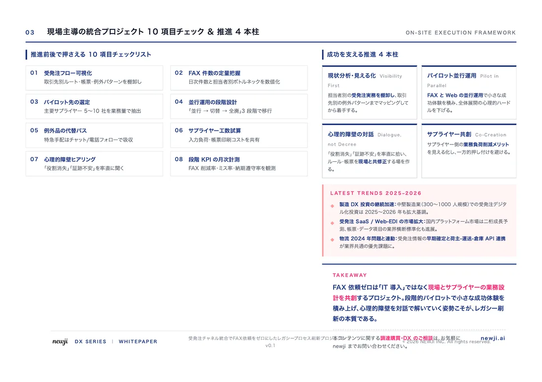
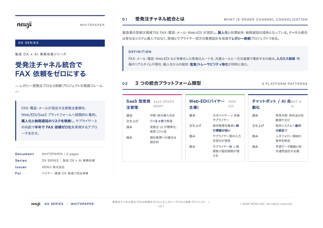
製造業の現場で使える実務資料(PDF)を無料でお届けします。"こんな資料が届きます" ↓ 下のボタンからどうぞ。
PRODUCT — 製造業向け 調達・受発注クラウド
この記事の課題、
newji で解決しませんか?
newji は、製造業の調達・受発注に特化したクラウド/AIエージェント。見積依頼・発注書作成・進捗管理・承認をひとつの画面に集約し、AIが比較と異常検知を担当。最後の「GO」だけ人が押す仕組みです。
- 見積〜発注〜納期を一元管理。催促・転記のムダをゼロに
- AIが相見積もり比較と異常検知。あなたは判断だけに集中
- 取引先は「招待」で完全無料。自社コストだけで取引先ごとデジタル化
※ 取引先から招待された企業様は完全無料でご利用いただけます


 調達購買アウトソーシング
 OEM/ODM 生産委託
 NEWJI DX
 受発注AIエージェント