

- お役立ち記事
- Basics of plasma CVD and its application to surface treatment and thin film creation

スタートアップから大手まで。
調達・受発注をAIで標準化。
相見積比較も進捗管理もAIが下支え。取引先は招待で完全無料。

Basics of plasma CVD and its application to surface treatment and thin film creation

目次
Understanding Plasma CVD
Plasma Chemical Vapor Deposition, commonly known as Plasma CVD, is a process extensively used in the field of materials science for creating thin films and treating surfaces.
It is a type of chemical vapor deposition which leverages plasma to enhance the reaction process.
This technique allows for the deposition of materials on substrates to a degree of precision and quality that other methods often cannot achieve.
Plasma CVD stands out due to its ability to produce uniform coatings.
The process operates under low temperatures and offers high deposition rates, making it versatile for various industrial applications.
How Plasma CVD Works
The Plasma CVD process begins with the introduction of gaseous precursors into a reactor.
These precursors are compounds that contain the elements to be deposited as a film.
A plasma is then generated by subjecting the reactor to a high-frequency electric field, which ionizes the gas molecules.
The presence of the plasma initiates a series of chemical reactions that result in the deposition of a thin film on the substrate surface.
Plasma not only speeds up chemical reactions but also facilitates the deposition on complex surfaces.
This is because the energetic species in the plasma can reach and react on surfaces with intricate geometries.
The precise control over the process parameters, such as gas pressure, power input, and temperature, allows for tailoring the properties of the deposited film according to specific requirements.
Applications of Plasma CVD
The applications of Plasma CVD are diverse and span across various fields, due to its capability to deposit a wide range of materials including metals, oxides, nitrides, and polymers.
Microelectronics
In the microelectronics industry, Plasma CVD is critical for creating thin films used in semiconductors.
These films are necessary for insulating, passivating, and protecting microelectronic components.
Thin film deposition through Plasma CVD ensures that the devices are efficient, reliable, and have long operational lives.
Optical Coatings
Plasma CVD is also key in producing anti-reflective and protective coatings for optical devices, such as lenses and mirrors.
These coatings enhance light transmission and protect the optical surfaces from environmental damage, thereby improving performance.
Surface Protection
In various industries, such as automotive and aerospace, Plasma CVD is employed to create protective coatings that enhance surface hardness and resistance to wear and corrosion.
These films substantially increase the durability of components that are subjected to harsh environmental conditions.
Biomedical Devices
The biomedical field benefits from Plasma CVD by using it to coat medical devices with biocompatible layers.
This improves the interaction between the device and biological tissues, enhancing the performance of implants and prosthetics.
Advantages of Plasma CVD
Plasma CVD offers several advantages over traditional CVD techniques and other deposition methods.
One of the main benefits is the ability to perform depositions at lower temperatures.
This is critical for substrates that are sensitive to high temperatures, helping prevent damage and preserving their structural integrity.
Plasma-assisted processes generally result in higher purity films due to the efficient reaction pathways.
This minimizes the incorporation of unwanted elements, leading to better quality coatings.
Furthermore, the process flexibility provides a high degree of control over the film properties.
This includes the ability to vary the thickness, morphology, and composition of the coat to meet specific needs.
Limitations and Challenges
Despite its benefits, Plasma CVD also faces certain limitations and challenges.
One notable challenge is the complexity of the equipment and the need for precise control over various parameters.
This makes the system setup relatively more expensive and maintenance-intensive than simpler deposition techniques.
Moreover, the dense and energetic nature of plasma can sometimes lead to the formation of defects or damage on sensitive materials.
Hence, understanding and controlling plasma interactions with substrates is imperative for ensuring optimal results.
Conclusion
Plasma CVD has established itself as a pivotal technology in the realm of material science and engineering due to its versatility and superior performance.
Its ability to form high-quality, uniform thin films makes it indispensable across industries including microelectronics, optics, automotive, aerospace, and biomedicine.
Despite its complexities, ongoing advancements in the understanding and manipulation of plasma processes promise to further enhance its application potential.
With continual research and development, Plasma CVD will likely remain at the forefront of innovation in thin film technology and surface treatment for the foreseeable future.
この記事の理解を深める
無料ホワイトペーパーをプレゼント
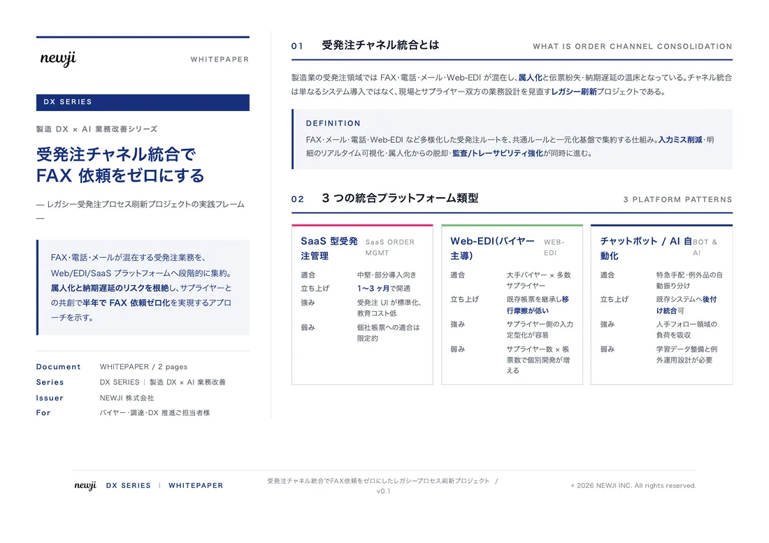
製造業の現場で使える実務資料(PDF)を無料でお届けします。"こんな資料が届きます" ↓ 下のボタンからどうぞ。

PRODUCT — 製造業向け 調達・受発注クラウド
この記事の課題、
newji で解決しませんか?
newji は、製造業の調達・受発注に特化したクラウド/AIエージェント。見積依頼・発注書作成・進捗管理・承認をひとつの画面に集約し、AIが比較と異常検知を担当。最後の「GO」だけ人が押す仕組みです。
- 見積〜発注〜納期を一元管理。催促・転記のムダをゼロに
- AIが相見積もり比較と異常検知。あなたは判断だけに集中
- 取引先は「招待」で完全無料。自社コストだけで取引先ごとデジタル化
※ 取引先から招待された企業様は完全無料でご利用いただけます




 調達購買アウトソーシング
 OEM/ODM 生産委託
 NEWJI DX
 受発注AIエージェント