

- お役立ち記事
- Basics and latest technology of semiconductor device packaging in the chiplet era

スタートアップから大手まで。
調達・受発注をAIで標準化。
相見積比較も進捗管理もAIが下支え。取引先は招待で完全無料。

Basics and latest technology of semiconductor device packaging in the chiplet era

目次
Understanding the Basics of Semiconductor Device Packaging
Semiconductor device packaging plays a crucial role in protecting and supporting electronic components.
It is the final stage of semiconductor device fabrication, providing a secure housing for the silicon chips.
Not only does packaging protect the chip from physical damage and environmental factors, but it also facilitates electrical connections to a circuit board.
The packaging process involves encasing the silicon die in a plastic, ceramic, or metal enclosure, and adding a lead frame or solder bumps to connect the chip to external circuits.
Over the years, there has been a continuous evolution in packaging technology to meet the demands of increasingly complex and high-performance devices.
Traditional packaging methods like Dual In-line Package (DIP) and Quad Flat Package (QFP) have given way to more advanced techniques.
These advancements are driven by the need for smaller, lighter, and more energy-efficient devices.
The Transition to Advanced Packaging
With the advent of technologies such as smartphones, tablets, and the Internet of Things (IoT), there’s been a significant push towards creating more efficient packaging solutions.
Advanced packaging technologies, such as Flip-Chip, Wafer-Level Packaging (WLP), and Through-Silicon Via (TSV), have revolutionized how semiconductor devices are encapsulated.
Flip-Chip packaging involves directly mounting the die onto the substrate by flipping it over.
This allows for a larger number of smaller and more closely spaced input and output connections, significantly improving performance and reducing size.
Wafer-Level Packaging (WLP) integrates the packaging process at the wafer level, before the die is cut.
This approach minimizes the need for large, individual packages, allowing for thinner and lighter designs.
WLP is particularly advantageous for mobile devices where space and weight are critical concerns.
Through-Silicon Via (TSV) technology introduces vertical electrical connections through the silicon wafer, allowing for three-dimensional (3D) stacking of chips.
This results in greater performance and functionality within a smaller footprint, ideal for high-performance computing applications.
The Emergence of Chiplets
The semiconductor industry is now entering what many refer to as the “chiplet era.”
Chiplets are small, functional chips that can be integrated into a single package to form a larger, more complex system.
They represent a shift from monolithic chip designs to modular architectures, offering various advantages including flexibility, cost-effectiveness, and improved performance.
In the chiplet approach, each chiplet performs a specific function, such as processing, memory, or interfaces, and can be mixed and matched to create tailored solutions.
This modularity allows manufacturers to quickly adapt to different market needs and technological advances.
Benefits of Chiplet Technology
One of the most significant benefits of chiplet technology is its ability to reduce production costs.
By breaking down large semiconductor designs into smaller, standardized components, companies can achieve economies of scale and run different chiplets on older, less expensive manufacturing nodes.
This design flexibility also enables rapid iterations of products.
Manufacturers can introduce new features or enhancements by simply swapping out specific chiplets, rather than redesigning an entire system.
Chiplet technology also aids in overcoming the limitations of Moore’s Law.
As we’re reaching the physical limits of shrinking transistor sizes, chiplets offer an alternative path to enhance performance by increasing the complexity and sophistication of system designs.
Furthermore, by distributing functions across multiple chiplets, thermal management becomes more effective, and power efficiency is improved.
The Role of Heterogeneous Integration
The emerging trend of heterogeneous integration is closely tied to the development of chiplet technology.
It involves the integration of different types of semiconductors and materials into a single package to perform various functions.
This approach marries the best features of different chip technologies, enabling superior performance and reduced power consumption.
Heterogeneous integration complements the chiplet strategy by allowing diverse chiplets, fabricated using different technologies, to work together within the same package.
This leads to more sophisticated systems capable of advanced computing, communication, and sensing tasks.
For instance, a package might contain chiplets for processing using FinFET technology, alongside optical chiplets for communication, and MEMS (Micro-Electro-Mechanical Systems) for sensing.
Challenges and Innovations in Packaging Technology
Despite the promising future, the chiplet era presents several challenges for semiconductor packaging.
The integration of multiple chiplets into a seamless system requires precise alignment and sophisticated interconnect technologies to ensure high bandwidth and low latency.
Furthermore, achieving compatibility among chiplets from different manufacturers is a significant hurdle that the industry must overcome.
Innovations such as Silicon Interposers and Embedded Multi-die Interconnect Bridge (EMIB) are emerging as solutions to these challenges.
Silicon Interposers provide a medium for high-density interconnects between chiplets, facilitating efficient communication.
EMIB, developed by Intel, is a cost-effective approach that uses a small silicon bridge to connect chiplets, reducing the complexity of packaging.
The Future of Semiconductor Device Packaging
In conclusion, the chiplet era represents a transformative phase in semiconductor device packaging.
As systems become more complex and diverse, the role of packaging will expand to integrate different technologies and materials in new and innovative ways.
The growth of chiplets and heterogeneous integration will drive the development of new packaging solutions, addressing challenges related to size, cost, performance, and thermal management.
As the industry moves forward, collaboration among chip manufacturers, foundries, and technology providers will be crucial in setting standards for compatibility and integration.
This collaborative effort will pave the way for the next generation of semiconductor devices that will continue to enhance the technological landscape across numerous fields, from consumer electronics to automotive, healthcare, and beyond.
この記事の理解を深める
無料ホワイトペーパーをプレゼント
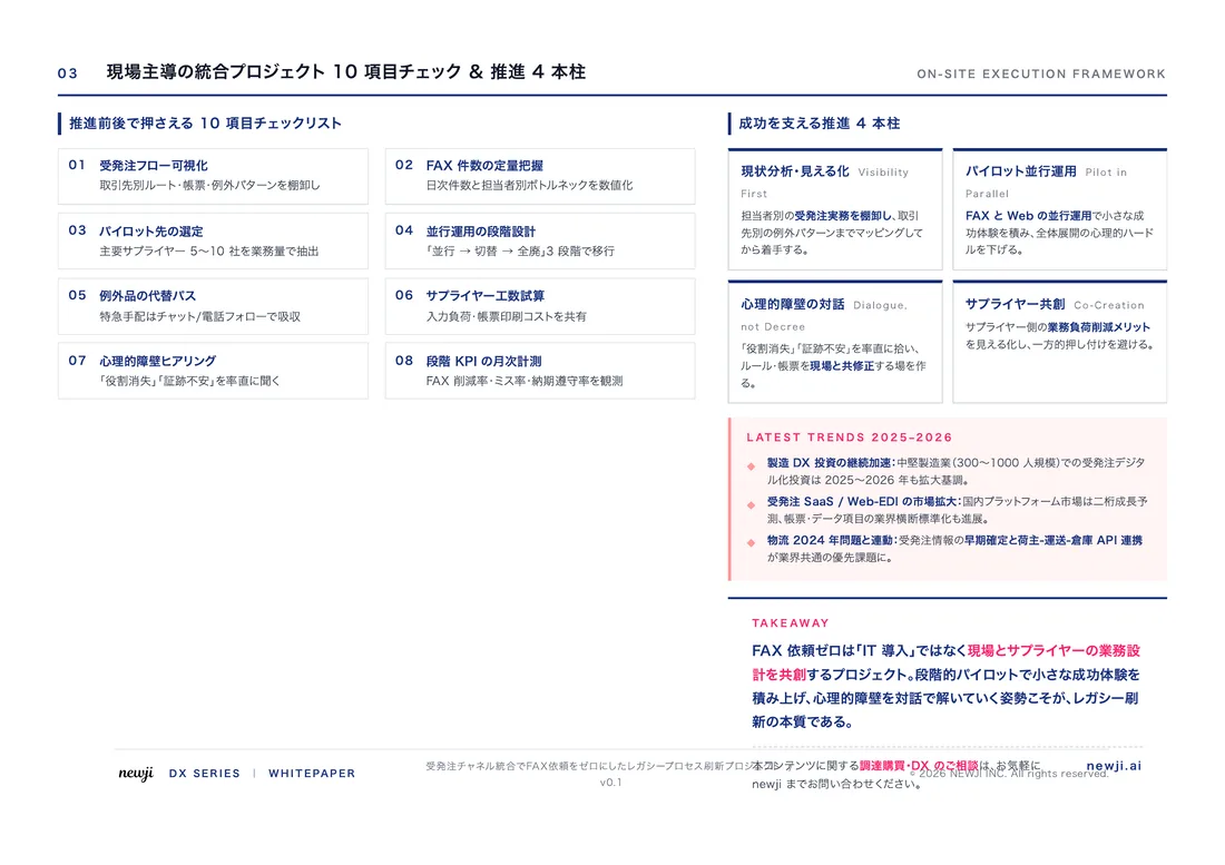
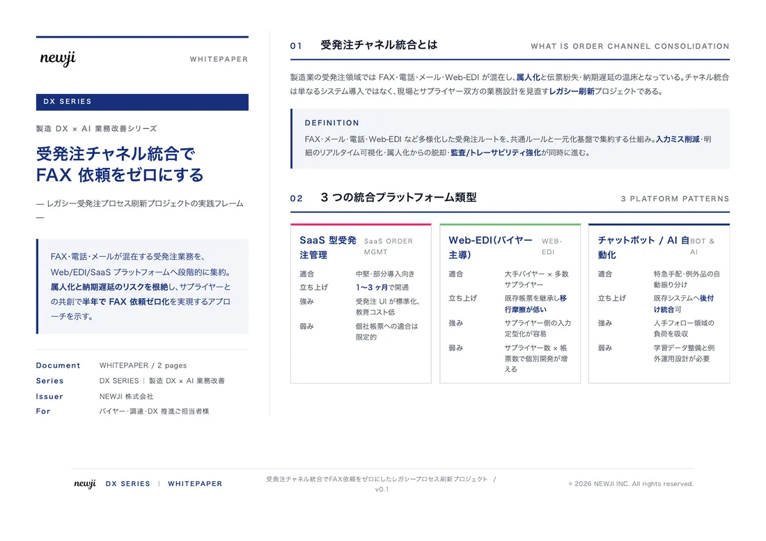
製造業の現場で使える実務資料(PDF)を無料でお届けします。"こんな資料が届きます" ↓ 下のボタンからどうぞ。
PRODUCT — 製造業向け 調達・受発注クラウド
この記事の課題、
newji で解決しませんか?
newji は、製造業の調達・受発注に特化したクラウド/AIエージェント。見積依頼・発注書作成・進捗管理・承認をひとつの画面に集約し、AIが比較と異常検知を担当。最後の「GO」だけ人が押す仕組みです。
- 見積〜発注〜納期を一元管理。催促・転記のムダをゼロに
- AIが相見積もり比較と異常検知。あなたは判断だけに集中
- 取引先は「招待」で完全無料。自社コストだけで取引先ごとデジタル化
※ 取引先から招待された企業様は完全無料でご利用いただけます
関連記事
-

Transforming Modern Electronics: Unleashing the Potential of Silicon-on-Insulator (SOI) Technology for Enhanced Industry Recognition and Market Expansion
-

Silicon Carbideを活用した次世代製造プロセスの最適化方法
-

半導体の小型高集積化に対応する次世代半導体パッケージの開発と最新技術
-
FOWLPの市場性から分類デザインプロセス応用将来まで全てを解説
-
3D実装技術の基礎と量産実用化に向けた多層配線技術の最新開発動向
-
半導体パッケージの基礎とSiP、WLP、FOWLP、TSVの最新技術
 調達購買アウトソーシング
 OEM/ODM 生産委託
 NEWJI DX
 受発注AIエージェント