

- お役立ち記事
- Fundamentals, State-of-the-art and Future Prospects of FOWLP Fan-Out Wafer Level Package

スタートアップから大手まで。
調達・受発注をAIで標準化。
相見積比較も進捗管理もAIが下支え。取引先は招待で完全無料。

Fundamentals, State-of-the-art and Future Prospects of FOWLP Fan-Out Wafer Level Package

目次
Understanding Fan-Out Wafer Level Package (FOWLP)
Fan-Out Wafer Level Package (FOWLP) is a modern semiconductor packaging technology that has gained popularity in recent years.
It stands out due to its ability to offer high performance, miniaturization, and cost-effectiveness compared to traditional methods.
To comprehend the fundamentals of FOWLP, it’s essential to grasp its basic structure and how it operates.
FOWLP involves the redistribution of input and output wires without using a substrate.
This means the silicon die is placed on a temporary carrier, encapsulated with molding compound, and then the redistribution layer (RDL) is applied directly onto the die and molding compound.
This process replaces the conventional need for a printed circuit board within the package, which enhances electrical performance and thermal dissipation.
Fundamentals of FOWLP
The Fan-Out Wafer Level Package technology was developed to improve the limitations of the Fan-In Wafer Level Package (FIWLP), enabling more significant functionality with fewer design restrictions.
The fundamental structure consists of a semiconductor chip, whose pins are relocated to outside the chip’s dimensions, facilitated by an RDL.
One of the critical components of FOWLP is the RDL, which acts as the connector between the semiconductor and the external world.
It allows for the redistribution of connections, ensuring they meet the density and design requirements.
The absence of a traditional substrate results in a slimmer and more reliable package.
Another foundational aspect is the use of a ‘molding compound’.
This material encapsulates the semiconductor chip and provides a reliable surface for the RDL.
It aids in protecting the chip from physical damage and enhances thermal management.
The outcome is a compact package with higher electrical performance and reduced thickness.
State-of-the-Art in FOWLP
In recent years, FOWLP has reached new heights with the advent of advanced techniques and applications.
One prominent development is the Enhanced FOWLP, which allows for the integration of multiple chips within a single package.
This capability is particularly useful in industries seeking to deliver sophisticated systems within compact dimensions, such as smartphones, IoT devices, and automotive electronics.
Another innovation is the heterogeneous integration capability of FOWLP.
This state-of-the-art advancement enables different types of chips, including analog, digital, and RF components, to coexist within one package.
It has driven the development of System-in-Package (SiP) solutions, offering immense flexibility in terms of electronic design and application.
High-Density FOWLP (HD FOWLP) is another ground-breaking innovation in the field.
It allows for increased I/O density through ultra-fine RDL features.
This advancement translates to even smaller packages, which remains a sought-after factor, especially in portable and wearable technology.
The result is enhanced functionality without compromising on device size or performance, addressing the growing demand for compact, efficient electronics.
Benefits of Using FOWLP
The advancements in FOWLP technology present several advantages.
Firstly, it provides excellent electrical performance due to the shortened interconnections and absence of a substrate.
This design results in lower parasitic inductance and resistance, leading to faster signal transmission and reduced power consumption.
Secondly, FOWLP offers impressive thermal management capabilities.
The encapsulation method using molding compounds provides an efficient path for heat dissipation, critical in high-performance applications.
As devices become more powerful, effective thermal management is crucial in maintaining reliability and longevity.
Furthermore, FOWLP enables significant size reductions in electronic devices.
Without the substrate, devices can be made thinner, which is critical in consumer electronics striving for sleek and portable designs.
This advantage helps manufacturers meet consumer demands for lightweight, compact gadgets without sacrificing functionality or performance.
Challenges in FOWLP Development
Despite its benefits, FOWLP faces specific challenges that require ongoing research and development.
One of the primary issues lies in its manufacturing complexity.
Precise placement and proper RDL fabrication demand advanced equipment and processes, increasing production costs.
Similarly, achieving high yield rates in FOWLP can be tricky.
The complexities involved mean that even minor issues can affect a batch, leading to potential wastage and economic loss.
Addressing these manufacturing nuances requires cutting-edge innovation and stringent quality control protocols.
Another hurdle is the thermal stress experienced by the packages.
While FOWLP does present better thermal performance, designing systems that manage thermal expansion and contraction efficiently remains crucial.
Thermal stress can potentially lead to mechanical failures, necessitating careful material and design consideration.
Future Prospects of FOWLP
The future of Fan-Out Wafer Level Package technology is promising, with ongoing research focusing on further innovations.
One potential direction is the proliferation of 5G and IoT technologies, which demand more sophisticated, miniature, and multi-functional devices.
FOWLP’s ability to integrate heterogeneous components makes it suitable for such advancements.
Moreover, developments in AI and machine learning applications call for robust, compact, and efficient computing solutions.
FOWLP can serve as the foundation for future AI chips, supporting the growing complexity and performance requirements of modern algorithms and applications.
Research also indicates a shift towards more eco-friendly and sustainable manufacturing processes.
The advancements in FOWLP packaging aim to minimize material waste and energy consumption during production.
These efforts align with global strategies for reducing the environmental footprint of technology production, moving towards a more sustainable future.
In conclusion, Fan-Out Wafer Level Package technology holds significant potential as industries continue to pursue miniaturization, increased performance, and better cost efficiency.
As advancements continue, the scope of FOWLP will expand, offering novel solutions to meet the needs of an ever-evolving technological landscape.
この記事の理解を深める
無料ホワイトペーパーをプレゼント
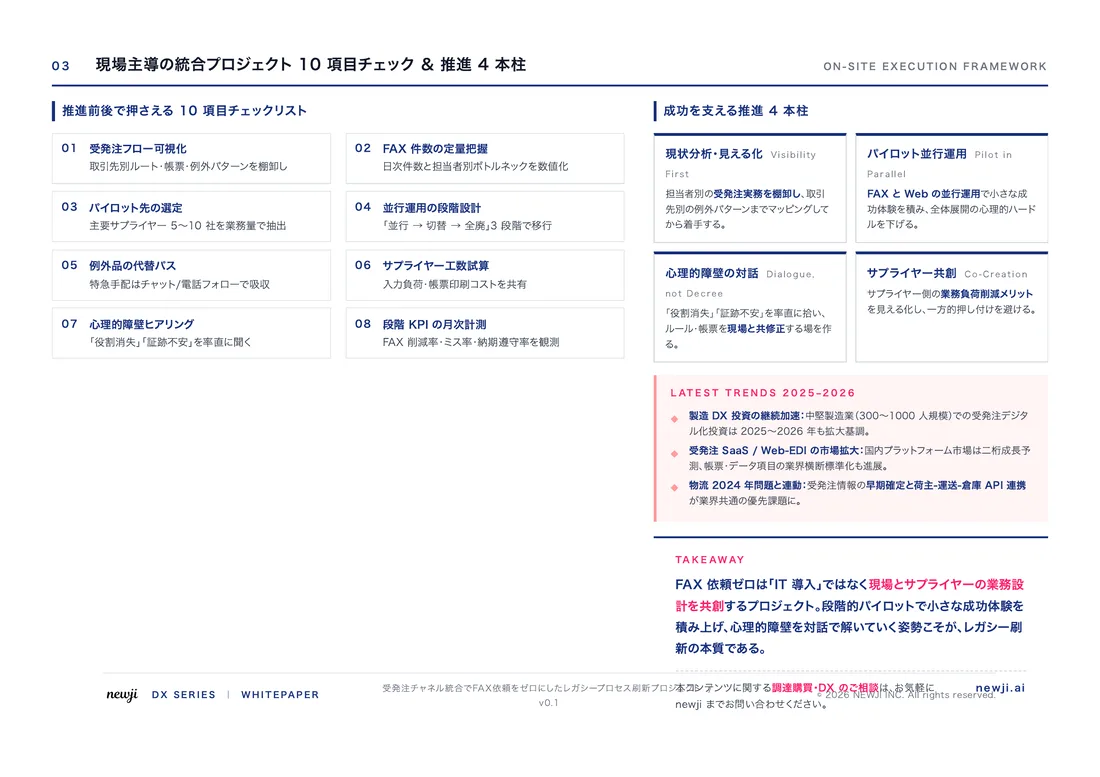
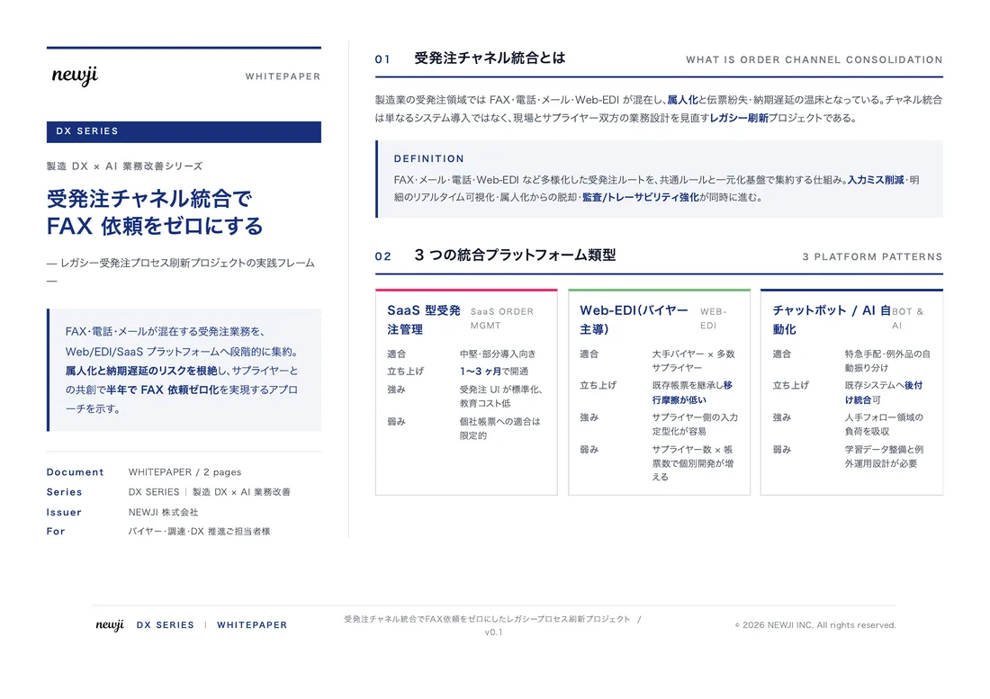
製造業の現場で使える実務資料(PDF)を無料でお届けします。"こんな資料が届きます" ↓ 下のボタンからどうぞ。
PRODUCT — 製造業向け 調達・受発注クラウド
この記事の課題、
newji で解決しませんか?
newji は、製造業の調達・受発注に特化したクラウド/AIエージェント。見積依頼・発注書作成・進捗管理・承認をひとつの画面に集約し、AIが比較と異常検知を担当。最後の「GO」だけ人が押す仕組みです。
- 見積〜発注〜納期を一元管理。催促・転記のムダをゼロに
- AIが相見積もり比較と異常検知。あなたは判断だけに集中
- 取引先は「招待」で完全無料。自社コストだけで取引先ごとデジタル化
※ 取引先から招待された企業様は完全無料でご利用いただけます
関連記事
-

FOWLPの市場性から分類デザインプロセス応用将来まで全てを解説
-
半導体パッケージの基礎とSiP、WLP、FOWLP、TSVの最新技術
-

Transforming Modern Electronics: Unleashing the Potential of Silicon-on-Insulator (SOI) Technology for Enhanced Industry Recognition and Market Expansion
-
FOWLPファンアウトウエハレベルパッケージの基礎と最新技術および将来展望
-
3D実装技術の基礎と量産実用化に向けた多層配線技術の最新開発動向
-
FOWLPファンアウトウエハレベルパッケージの基礎と最新技術

 調達購買アウトソーシング
 OEM/ODM 生産委託
 NEWJI DX
 受発注AIエージェント